Crack Formation during Electrodeposition and Post-deposition Aging of Thin Film Coatings - 1st Quarterly Report
First Quarterly Report - AESF Research Project #R-118. This new NASF-AESF Foundation research project report covers the First quarter of project work (January-March 2016).
#nasf
by
Prof. Stanko R. Brankovic*
Featured Content
University of Houston
Houston, Texas, USA
Editor’s Note: This NASF-AESF Foundation research project report covers the first quarter of project work (January-March 2016) on this new project at the University of Houston. A printable PDF version is available by clicking HERE.
Objective
The objective of this work is to study fundamental and practical aspects of crack formation in electrodeposited thin films. The aim is to identify and quantify key parameters of the electrodeposition process affecting the crack formation in thin films. This study should enable development of an effective strategy generally applicable in practice whenever electrodeposition process for crack free films is demanded.
The activities performed in this period are focused on initial studies of electrodeposition of chromium thin films of arbitrary thickness on copper, gold and nickel polycrystalline substrates from Cr+3-containing electrolytes. The bath formulation for this work is based on standard Cr+3 baths developed by Faraday Technology (Clayton, Ohio), labeled as EX DBA 1411 and EX DBA 1318 in Table 1. The first experiments were set to explore experimental boundaries of both bath systems, and to test the proposed experimental approach for detecting the onset of crack formation in chromium films.
Table 1 - Operating parameters of trivalent chromium baths under study.
| Designation | j (mA/cm2) | pH | T (°C) |
| EX DBA 1411 | 250-450 | 5.2-5.4 | 35 |
| EX DBA 1318 | 250-450 | 2.5 | 27-54 |
Experimental approach
The current understanding of crack formation in chromium films identifies the high stability of Cr+3 in water as a root cause. The Cr+3 forms a strong complex with water molecules. This causes its solubility at the interface to be strongly dependent on interfacial pH (pHi) having a great tendency to form an insoluble hydroxide.1 The precipitation of the oxide phase on the growing metal surface during electrodeposition results in incorporation of amorphous oxide phase at the grain boundaries.2 This is expected to negatively effect the fracture toughness of chromium films. The overall effect of oxide phase incorporation is manifested through the increased oxygen content in the chromium films and crack formation as a consequence of reduced fracture toughness, and/or oxide particles acting as stress concentration inhomogeneity. To study this phenomenon it is of crucial importance to accurately identify the critical thickness of chromium-films at which the onset of crack formation starts. In our work we proposed several in situ methods to identify the moment of crack formation in chromium films during electrodeposition process. The initial work on their implementation is described in proceeding text.
In situ measurements of stress evolution in chromium films
The most important part of the characterization work represents in situ measurements of stress-thickness and stress-time evolution and identification of the crack formation/propagation moment in chromium films. At the same time, this allows one to identify the critical thickness of the chromium film for crack formation which is important parameters for phenomenological description of the crack formation process.
These measurements will be performed using cantilever bending method.3 For this purpose our in-house system has been modified and re-fitted with a 10 mW laser, and custom cantilever holder system (Fig. 1). The main parts of the system are labeled in Fig. 1(a), indicating the laser path though the beam splitter, electrochemical cell, position sensitive detector (PSD), PSD-signal amplifier and laser beam focusing iris. The custom designed electrochemical cell is positioned on a special stage that can be adjusted in terms of the height and inclination along two axes parallel to the path of the laser beam. This allows one to acquire the best possible tuning of the laser reflection to the center of the PSD, which is mounted on an X-Y stage, allowing the position change with micrometer precision.
The fully mounted cell with all elements, except the solution, is shown in Fig. 1(b), with laser reflection from the back side of the cantilever. The front side of cantilever is deposited with a gold, nickel or copper thin film facing the counter electrode. This means that the laser reflection is from the glass cantilever side that is not affected by the chromium deposition and thus the reflection of the laser beam does not change in intensity as the chromium film is grown on top of the gold, nickel or copper seed on the front side. The volume of the cell is 150 mL which is sufficient for most of the experiments without fear that conditions in the solution will change during chromium thin film growth.
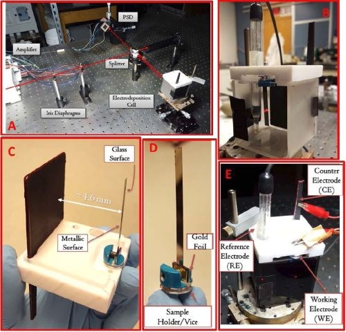
Figure 1 - The most important details of the in situ stress measurement system at the University of Houston: (a) overall system with some of the most important parts labeled, (b) electrochemical cell without solution with Au-deposited glass cantilever, reference and counter electrode, (c) rigid cell holder made of Teflon to which the cantilever vise and fixture, counter electrode and reference electrodes are rigidly attached. The distance between the counter electrode and cantilever/working electrode is indicated as well as the side of the cantilever where Au or Ni is deposited, (d) custom made vise/fixture providing a rigid positioning of the glass cantilever and contact to the Au thin film deposited on the inner side of the cantilever, (e) cell with Cr+3 solution and all other details ready for measurements. The laser spot reflection from the outer side of the cantilever to the PSD is visible as a red dot on the right hand side. The second red spot is the laser reflection from the beam splitter to the wall of the cell.
In Fig. 1(c), an upside-down view of the Teflon holder with the cantilever fixture and counter electrode mounted are shown, indicating clearly which side of glass cantilever is deposited with gold. It also shows the distance between two electrodes. This distance can be adjusted by moving the counter electrode closer to the cantilever while keeping their mutually parallel arrangement intact. The area of the counter electrode is about 20 times larger than the area of the working electrode which prevents any kinetic limitation for deposition on the anode side, and also minimizes gas evolution on the anode. The primary current distribution in the cell has been verified in previous work and found to be very good. Uniform films of CoFe were grown routinely in this cell with this electrode arrangement.4
We have paid special attention to the design of the holder/cover of the cell in the area where the cantilever vise/fixture is attached. The Teflon cap itself is machined to provide a perfectly rigid match to the walls of quartz cell body, so that a tight seal and very rigid and stable mounting is achieved. In addition, the position of the Teflon holder is further stabilized by clamping the holder to the cell, Fig. 1(e). At the position where the cantilever holder is placed, the wedge is machined in the Teflon holder, Fig. 1(c), so that the metal part of the cantilever vise can have clearance above the cell walls, and thus allow the cantilever position to be as close as possible to the cell walls. This minimizes the path that laser beam passes through the solution and thus, ensures sufficient intensity of the reflected laser beam to the PSD, even for the dark Cr+3 solution as shown in Fig. 1(e). The metal vise to which the cantilever is fixed is machined in our shop and is shown in Fig. 1(d). The tightening of the cantilever to the vise is achieved by special screw. The gold foil is added to the design of the one leg of the vise so that contact to the glass film on the gold side is better, and more uniform clamping of the cantilever is achieved. The holder is attached to the Teflon cap body with the pin that is inserted in the Teflon cap and to which electrical contact is made, Fig. 1(e).
One of the issues that had to be addressed at the very beginning was the maximum length of the laser beam path through the solution that would still yield a reasonable and useful signal-to-noise ratio (SNR) to allow precise measurements. Before machining all parts of the cell, several studies were made to measure the attenuation of the laser beam on the position sensitive detector (PSD) as a function of the length of the laser path through the Cr+3 solution.
The basic concept of the experiment is shown in Fig. 2 where the main parts of the set-up are described. The glass slides with variable thickness, i.e., the thickness of the Cr+3 solution layer, were custom made in our lab. Using these slides as etalons,** the attenuation of the laser intensity was investigated, and the signal-to-noise ratio obtained from the PSD was evaluated.
The complete set of data obtained in this study is shown in Table 2. We have compared the SNR of the signal with the extraneous noise coming from mechanical vibrations, inherent laser intensity fluctuation and thermal noise from electronics and signal with the additional effect of attenuated intensity due to solution absorption as a function of solution layer thickness. It was determined that a solution layer thicker than 2 mm cannot be allowed in order to have meaningful and sensitive in situ stress measurements.
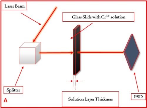

Figure 2 - (a) Basic set-up for measurements of the laser beam intensity attenuation as a function of the length of laser beam path through the Cr+3 solution. These measurements were done using the same set-up as for the in situ stress measurements. The example of the signal transient recorded on position sensitive detector (PSD) and corresponding signal-to-noise ratio (SNR) for laser beam passing through the Cr+3 solution layer with (b) 3 mm and (c) 1 mm thicknesses are shown for illustrative purposes.
Table 2 - Results of laser beam intensity attenuation studies.
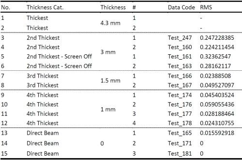
This means that maximum distance between the back of the cantilever from which the laser reflection has to occur to the PSD and the wall of the cell for in situ stress measurements can be only 1 mm. With this in mind, we proceeded with machining the Teflon holder for our cell and vise-fixture for our cantilevers.
The first successful in situ measurements of stress evolution during chromium electrodeposition have been performed. The solution tested was EX DBA 1411 with a current density of 250 mA/cm2. The preliminary data are shown in Fig. 3 which indicated that our laboratory set-up is capable of measuring stress evolution in chromium films despite very challenging conditions of solution absorbance. The data in Fig. 3(a) show the stress-thickness curve and the inset in Fig. 3(b) shows the electrochemical cell during measurements with the laser spot reflected on the PSD coming from the cantilever. The chromium film thickness in this figure is not measured, but calculated from current data, assuming the current efficiency of 100%. This is not absolutely correct. Therefore, these data serve only for illustrative purposes, demonstrating the capability of our measurement set-up rather than for any quantitative and qualitative analysis.
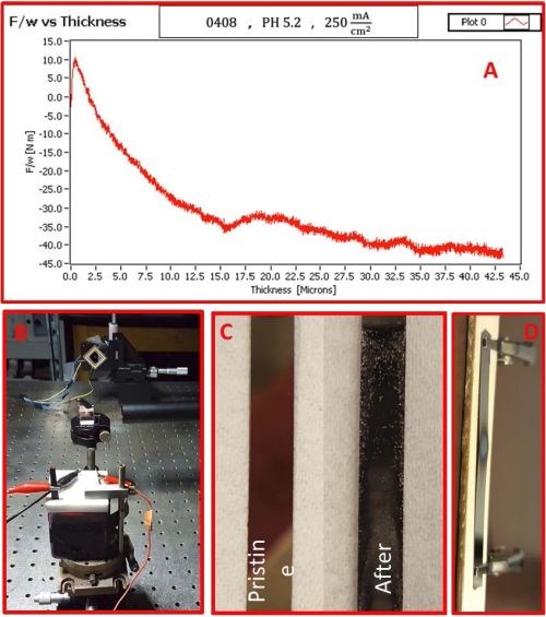
Figure 3 - (a) stress-thickness evolution during the deposition of chromium film from EX-DBA 1411 bath at j = 250 mA/cm2, (b) the electrochemical cell and laser beam reflection on the PSD during stress measurements, (c) pristine gold surface and chromium-deposited on gold-coated cantilevers during stress measurement, (d) example of excessive heating of the gold seed on glass cantilever leading to the seed failure.
During in situ stress measurements several issues have been encountered. The first one is the dull appearance of the chromium deposit that did not seem to have uniform coverage of the cantilever (Au-seed, Fig. 3(c)). We have investigated this problem in more detail, and found out that the reason is excessive heating of the 100 nm thick gold seed layer in the very beginning of chromium electrodeposition. The thickness of the gold film acting as a seed in these preliminary in situ stress measurements was 100 nm. This yields the cross-section of the seed that carries the applied 250 mA deposition current to be 10-5 cm (film thickness) × 0.4 cm (film width). Therefore, the current density through the cross-section area of the gold seed is 6.25 × 10⁷ mA/cm2. Such current densities at the very beginning of the deposition could lead to excessive heating of the seed layer and local overheating of the solution in the contact with the surface of the cantilever. In fact, our test experiments with the cantilever fixture mounted in air and passing the same current caused failure of the seed, i.e., seed-burnout after just a few minutes, as in Fig. 3(d). The excessive heat generated by Joule heating resulted in peeling of the seed due to the huge thermal stresses developed between the glass and Au/Ta seed layer. We think that the same scenario was responsible for non-uniform chromium film evolution morphology. To offset this problem, we are now developing a new cantilever with a nickel seed layer which is between 1 and 2 microns in thickness. This should prevent excessive heating of the seed, and result in a more stable and uniform chromium deposit morphology evolution on the cantilevers, and therefore, a more controlled in situ stress measurement.
In situ impedance measurements during chromium deposition
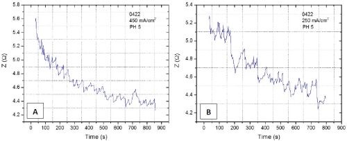
Figure 4 - Z vs. time plot obtained during chromium electrodeposition on a copper seed for (a) j = 450 mA/cm2 and (b) j = 250 mA/cm2. The amplitude of perturbation current is 3 mA/cm2 and the frequency is 10 kHz.
The complementary experiments to in situ stress-thickness and stress-time evolution we intend to perform are the in situ electrochemical impedance spectroscopy measurements (EIS). The idea is to monitor the impedance of the system during chromium deposition and develop methodology that would be sensitive to detect the onset of the crack formation and crack propagation. The ultimate goal is to develop an experimental routine where we could have a simultaneous measurement of stress and impedance in parallel. In our preliminary trials, we have run several deposition experiments using EX DBA 1411 bath chemistry at j = 250 mA/cm2 and 450 mA/cm2 and with a current modulation of 3 mA/cm2 having different frequencies of perturbation. An example of the impedance data recorded in two separate experiments is shown in Fig. 4. At this stage, we are still investigating the chromium deposition system to see at which frequency the impedance change is the most sensitive to the onset of crack formation and crack propagation. With more data, we will be able to start developing a phenomenological model that would be used for quantitative analysis of impedance data, and their interpretation in terms of crack density, depth, onset of formation, etc.
Chrono-potentiometric studies of the chromium deposition process
This work will focus on correlating the interfacial stability for Cr(OH)3 precipitation during chromium electrodeposition with the critical thickness for chromium thin film cracking. The aim is to find evidence for a fundamental link between the hydroxide incorporation phenomenon and resulting crack formation in chromium thin films. As a first step in this study we have done experiments investigating the potential of the chromium surface as a function of deposition current density in the range of the operating parameters of each bath. The experimental set-up for these measurements closely matches the one used for in situ stress measurements in terms of electrode area, distance, geometry and contact resistance etc., in Fig. 5(c-e). Several sets of experiments have been completed and the summary data for each bath are shown in Fig. 5(a,b). As is evident, the resting potential of the growing chromium surface during deposition under galvanostatic conditions is a linear function of applied current density for each bath (mixed control). Higher current densities lead to a more negative potential on the electrode surface which is, in each case, always <-1.4 VSHE. The potential range that corresponds to investigated current densities is also plotted in the Pourbaix diagram shown in Fig. 6. One can see that the bath with higher pH (EX DBA 1411, pH = 5.2) also has a more negative resting potential during chromium growth in the current density range between 250-450 mA/cm2. Considering that one of the parasitic reactions is hydrogen evolution: 2H+ + 2eˉ = H2, occurring in parallel with chromium deposition, this is not surprising. One can anticipate a much larger contribution of concentration polarization due to this reaction to the overall potential of the chromium surface at condition of high pH. Therefore, the dE/dj differences between the data for EX DBA 1411 (-4 V/A) and EX DBA 1318 (-0.75 V/A) can be attributed to the same effect. A confident analysis of these data awaits a full disclosure of the proprietary bath chemistries.
One of the goals of our study is the accurate determination of interfacial pH values for each solution/deposition process. They can be calculated from literature data (formate-Cr+3 complex stability constant and Cr(OH)3 solubility product), solution parameters (bulk pH, calculated concentration of Cr+3 at the interface), and experimental measurements (current efficiency, chromium deposition rate).2 However, this formulation has to be revisited in more detail. The reason is that, at this point, we have to appreciate the fact that both chromium deposition baths operate at potentials that are more negative than the electrochemical water reduction reaction, as in Figs. 5(a,b) and 6: 2H2O + 2eˉ = H2 + 2OHˉ. Therefore, having water as the most concentrated reactant in the solution, ~55 M, we have water reduction as the dominant reaction at the interface, not limited by transport, and also producing OHˉ. This effect is significantly more important for interfacial pH than the H+ reduction and therefore we intend to derive a new model for the calculation of interfacial pH to accommodate this fact. However, as a first approximation, one can assume that the interfacial pH during chromium electrodeposition is very high, perhaps >>14. At this interfacial pH value, one can see that the Cr(OH)3 is a stable phase which precipitates (Kp~10-31) and incorporates in the chromium deposit, as in Fig. 6. This is an indirect indication that control of the Cr(OH)3 precipitation is a key to achieve crack-free chromium deposits.
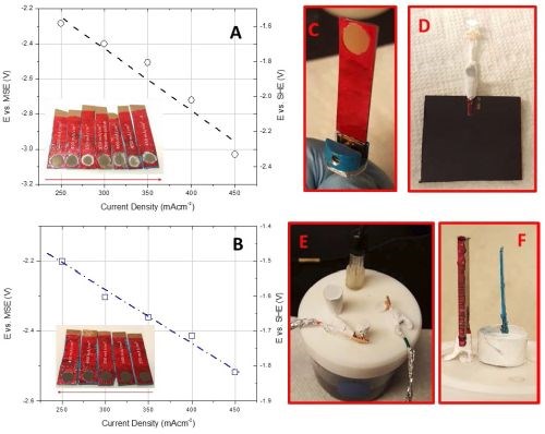
Figure 5 - Results from chrono-potentiometric studies of chromium deposition for (a) EX DBA 1411 bath and (b) EX DBA 1318 bath; (c) fixture for the copper sample with the defined area of the working electrode, (d) counter electrode, (e) electrochemical cell for chrono-potentiometric studies and (f) geometric arrangement of the counter and working electrode. All parts of the experimental set-up closely resemble the one for in situ stress measurements shown in Fig. 1.
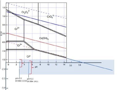
Figure 6 - Pourbaix diagram for chromium amended by the author to illustrate the effect of very high pH at the interface induced by electrochemical water reduction reaction. The potential range of each bath is indicated for the current density range investigated. The extended range of pH is projected to emphasize the possibility of Cr(OH)3 precipitation.
Summary
The activities in this first quarter focused on establishing a reliable experimental methodology to measure and identify the moment of crack formation in chromium electrodeposition, and to evaluate the conditions at the electrochemical interface for Cr(OH)3 precipitation and incorporation. At this stage, our future efforts are planned to produce reliable cantilevers which will result in reproducible and accurate stress-thickness and stress-time evolution measurements during chromium deposition. Fulfillment of this goal provides the next step towards establishing the methodology for crack formation identification. Our efforts in the development of complementary impedance measurements will focus on determining the optimum frequency of the current perturbation at which the onset of crack formation in chromium films is easily detected. More work is necessary to determine this optimum experimental condition. A current booster unit will be acquired which will allow impedance measurements with currents higher than 100 mA, and thus work with real size cantilever electrodes as they are employed in the in situ stress measurement set-up. The final goal of the experimental development is to design a simultaneous in situ stress and impedance measurement system that will be capable of an unambiguous detection of crack formation in chromium films. The progress in understanding the conditions at the electrochemical interface with respect to interfacial pH values and formation/precipitation of Cr(OH)3 will continue with the aim of determining an accurate partition of the deposition current corresponding to true Cr+3 reduction reaction.
References
1. M. Pourbaix, Atlas of Electrochemical Equilibrium in Aqueous Solutions, NACE International Cebelcor, Houston (1966); p. 256.
2. S. Elhalawaty, et al., J. Electrochem. Soc., 158 (11), D641-D646 (2011); see also J. George, et al., Electrochimica Acta, 110, 411-417 (2013).
3. L.B. Freund and S. Suresh, Thin Film Materials: Stress, Defect Formation, and Surface Evolution, Cambridge University Press, (2003); p. 283.
4. S.R. Brankovic, et al., Electrochimica Acta, 83, 387-393 (2012).
Footnotes
*Corresponding author:
Dr. Stanko R. Brankovic
Associate Professor
Department of Electrical & Computer Engineering
Department of Chemical & Biomolecular Engineering
Department of Chemistry
N 308 Engineering Building 1
Houston, Texas 77204-4005
Phone: (713) 743-4409
Fax: (713) 743-4444
E-mail: srbrankovic@uh.edu
**Etalon - a device consisting of two reflecting plates for producing interfering light beams.
About the author:

RELATED CONTENT
-
PFAS and the Surface Finishing Industry
NASF and its member companies have a long history of environmental stewardship, especially when it comes to PFAS.
-
Development of a Sustainability Metrics System and a Technical Solution Method for Sustainable Metal Finishing: AESF Research Project #R-121, 6th Quarterly Report
The NASF Research Board has funded a research grant at Wayne State University on sustainability in the surface finishing industry, under the direction of Professor Yinlun Huang. The objective of the work is to create a surface-finishing-specific sustainability metrics system to measure economic, environmental and social sustainability. In this report, a benchmarking study of five plants was undertaken to illustrate how the sustainability assessment works.
-
Plastics and Plating on Plastics [1944]
This republished 1944 AES convention paper presents an historic perspective of the early days of plastics in surface finishing - using them and plating on them, in the waning years of World War II. The discussion reviews the uses of plastics in plating equipment and processing at that time, as well as the coating of the plastics themselves, with accompanying application photos. You will note that today’s conventional plating-on-plastics processes lay far in the future. Surprisingly, CVD processes are discussed.


