Designer EN
Post treatments can tailor properties of electroless nickel deposits
Electroless nickel has enjoyed a tremendous amount of growth as an engineering coating since its discovery more than 60 years ago. EN’s unique combination of deposit properties, including hardness, wear resistance, corrosion resistance, low porosity and non-magnetic characteristics, as well as its ability to deposit a uniformly thick layer over the surface of complex components, make it a popular choice as a functional coating for applications in the aerospace, automotive, computer, electronics, food, textile, and oil and gas industries.
As-plated electroless nickel has found great acceptance. But a number of post-plating processes can be used in combination with EN to develop or enhance a variety of properties.
Featured Content
These include post-dips, heat treatment, top plates, grinding and polishing, soldering, painting, blackening, and brazing. Combining these processes with EN can improve quality, performance and product life, ensuring that EN will continue to find more opportunities to solve old problems and provide answers to new technological hurdles.
Post-Dips
Post-dips are frequently used after electroless nickel plating to passivate the EN deposit, reduce the tendency of the deposit to stain and increase the corrosion resistance of the plated part by minimizing porosity in either the EN film or the substrate. Common post-dips include chromates, organics, and silicates.
Chromates
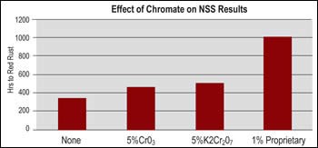
Typical con-centrations and operating conditions for a chromate post-dip treatment are potassium dichromate at a concentration of 10–30 g/L, temperature of 75–140°F, and time of 2–5 min. Such a chromate post dip does an excellent job of passivating the EN deposit and minimizing staining when parts are dried. For steel and aluminum components, chromates effectively passivate any substrate areas that may be exposed due to part imperfections or deposit porosity.
An issue with use of chromate post dips is the recent implementation of RoHS and other environmental and worker safety directives which have either restricted the use of hexavalent chromium (Cr6+) by setting a limit of 1,000 ppm of Cr6+ on the plated part or have banned the intentional use of Cr6+ anywhere in the plating process. Use of trivalent (Cr3+) chromates can minimize or eliminate problems associated with Cr6+ from either an environmental or worker safety standpoint.
Organic Post-Dips
In response to RoHS and other directives, some of the first alternatives to chromate passivation are organic-based post-dips. These are solutions borrowed from the electronics industry’s organic solderability preservative technology, which basically deposits a thin organic film over the entire surface of the part.
Organic post dips have shown the ability to increase the corrosion protection of the untreated part slightly, but not to the same extent as the chromating solutions. The major drawback of these systems is their tendency to cause a lot of staining, which is difficult to handle in high-volume production applications. Despite this, organic post-dips are currently used because of their non-chrome nature.
Silicates
Post-dip solutions of silicates can also be used to slightly increase the corrosion protection of electroless nickel films. These solutions contain soluble silicates which react with any anodically polarized areas on the part surface, such as exposed iron or aluminum, to form a protective silicate film. The increase in protection from these films is marginal and temporary, and in many applications the presence of the silicate residue is detrimental to part performance.
| Table 1 - Process parameters for heat treatments used on EN deposits | |||
| Class | Description | Temperature, °C | Time, hr |
| 1 | As Plated | ||
| 2 | Heat treatment for maximum hardness | ||
| Type I | 260 | 20 | |
| 285 | 16 | ||
| 320 | 8 | ||
| 400 | 1 | ||
| Type II | 350-380 | 1 | |
| Type III | 360-390 | 1 | |
| Type IV | 356-400 | 1 | |
| Type V | 375-400 | 1 | |
| 3 | Hydrogen embrittlement and adhesion on steel | 180-200 | 2-4 |
| 4 | Adhesion, carburized steel and age- hardened aluminum | 120-130 | 1-6 |
| 5 | Adhesion on beryllium and aluminum | 140-150 | 1-2 |
| 6 | Adhesion on titanium | 300-320 | 1-4 |
Heat Treatment
Electroless nickel’s wear resistance is greater than that of most typical electrolytic deposits due to its higher “as-plated” hardness. As-plated hardnesses for typical low-, mid-, and high-phosphorus EN deposits are 600–700 HV100, 500–550 HV100, and 450–500 HV100, respectively.
The deposited EN coating can be heat treated after plating to further increase hardness and actually rival the hardness of hard chrome. Hardnesses for heat-treated EN are in the range of 950 HV100; hard chromium is near 1050 HV100. The advantage in this case is that one gets nearly the wear resistance of chromium while enjoying the corrosion resistance and coverage of EN—and eliminating the potential headaches associated with chromium use.
It should be noted that the corrosion resistance of EN does decrease as a result of heat treatment. This is due to the reaction of nickel with phosphorus and the resulting precipitation of nickel phosphide crystals. This process also causes the EN deposit to shrink. The results are crystal grain boundaries along which corrosion can propagate and microcracking of the deposit.
Heat treatment after electroless nickel is also used to improve adhesion on certain alloys or to provide relief from hydrogen embrittlement.
This last application requires Class 3 heat treatment performed preferably within one hour of plating but not more than three hours post-plate. ASTM B 733-04 outlines the various classifications and conditions of post-plating heat treatment. ASTM B 850-982 provides more detailed information on hydrogen embrittlement relief. Table 1 outlines processing conditions for the various classes of EN heat treatments.
When heat treating EN-coated parts at temperatures above approximately 600°F (315°C), an inert (nitrogen or argon) or reducing (hydrogen) atmosphere should be used to prevent darkening due to heavy oxidation of the deposit. Heat treating at excessive temperatures or times will also result in subsequent softening of the hardened EN deposit due to grain coarsening.
Plated Top Coats
In many applications, EN can be combined with an electroless or electrolytic top coat of another metal to greatly improve part functionality by combining the desirable properties of several different deposits. As an undercoat, EN finds use because of its ability to evenly cover and protect all surfaces of a part, including blind holes and deep recesses. It also acts as a diffusion barrier between mutually soluble metals. Table 2 lists some examples of the metals used over EN and their applications.
Machining
Even though electroless nickel evenly covers the surface of a part and can be held to tight thickness tolerances, there are applications where some type of post-plate machining is required. Several machining techniques can be used, including grinding, precision turning and, when the application demands a very smooth, flat surface, chemical mechanical planarization (CMP).
| Table 2 - Typical Plated Top Coats Used Over EN | |
| Topcoat | Application Property |
| Hard Chromium | Wear resistance |
| Copper/Nickel/Chromium | Decorative |
| Zinc | Sacrificial corrosion resistance |
| Cadmium | Sacrificial corrosion resistance |
| Silver | Microwave |
| Immersion Gold | Solderability |
| Electroless Gold | Gold wire bonding |
| Electrolytic Gold | Infrared reflector, electrical contacts |
| Tin | Solderability |
Post-plate grinding of EN deposits is very common in industries such as aerospace, where critical parts are made of very costly materials and re-use of components is desirable to maximize part life at a reasonable cost. This is accomplished through over-plating the worn part with EN (also used for its desirable physical properties), then grinding the deposit back to the original component dimensions. High-phosphorus EN deposits are typically the coatings of choice for these applications because of their higher degree of ductility, compressive stress, and ability to build to very high thicknesses.
Diamond turning or precision machining is another process used to post-finish EN deposits. This process uses a hard, sharp, single-point diamond tool and extremely precise turning machines to produce finished or nearly finished optical surfaces with overall part tolerances of at least 10 μinches (0.25 μm). High-phosphorus electroless nickel deposits are again the coatings of choice for these applications because of their ability to be machined to an excellent finish. They also produce the least amount of wear on the diamond tool and provide long tool life.
Chemical mechanical planarization (CMP) is a more advanced technique for polishing materials such as EN deposits to create a very smooth, flat surface. The process combines the chemical removal effect of an acidic or basic solution with the mechanical effect of polishing with an abrasive material. Typically, CMP consists of a polishing head which presses the substrate against a flexible pad. While the polishing head is non-concentrically rotated, a chemical slurry is introduced between the substrate and pad. The result is material removal to form a very planar surface with Angstrom levels of finish. CMP is commonly used in the microelectronics and hard disk drive industries.
Soldering
In the electronics industry, soldering of EN-plated electronic components is a very common assembly operation. All electroless nickel coatings are solderable. The keys to successful soldering are understanding the differences between various EN deposits, post-plate handling and storage and matching the correct flux to the EN system in use.
Immediately after plating, low-phosphorus electroless nickel is the most solderable, followed by mid-phosphorus, and finally high-phosphorus deposits. This is due to the fact that the lower the phosphorus content of the deposit, the more nickel there is available to form a bond with the solder and the slower the deposit passivates.
Unfortunately, this advantage disappears within a relatively short period of time—generally no more than several hours. Because of their relatively high nickel content and the codeposition of various impurities such as sulfur, low- and mid-phosphorus EN deposits develop a much thicker oxide film than high-phosphorus deposits, making them more difficult to reactivate.
Post-plate handling, including final rinsing, drying, and packaging, plays a very large role in an EN-plated part’s solderability. It is imperative that parts be thoroughly rinsed in high-quality DI water, efficiently dried, and quickly removed from the shop environment. After parts are allowed to equilibrate to room temperature in a protected environment, they should be packaged in plastic bags back-filled with dry nitrogen and/or desiccant packs. This will slow oxide film growth on the EN surface. If baking is required prior to packaging, it should be done in a nitrogen or argon atmosphere.
Once packaged, storage time and conditions need to be considered. In general, time in storage should be kept as short as possible, and the storage conditions should be under low temperature and humidity.
During soldering, it is critical that the correct flux be used to properly deoxidize and clean the surface of the EN deposit. For electronic components, users are limited to the rosin-type fluxes. This is due to the corrosive nature of the inorganic acid and salt-based fluxes. There are three basic types of rosin fluxes:
• R, or non-activated, rosin
• RMA, or rosin mildly activated with organic acid hydrochlorides
• RA, or rosin activated with zinc chloride (ZnCl2)or ammonium chloride (NH4Cl).
The R-type flux, which might be sufficient for a freshly plated deposit, is not strong enough to clean, deoxidize, and activate an aged EN surface. These fluxes are meant for use on easily soldered surfaces like tin. RMA-type fluxes are more commonly used for soldering EN coatings, because the organic acids added to these fluxes can remove the oxide film formed on the EN surface. If the oxide film is too thick, however, soldering will be difficult. RA-type fluxes can also be used for soldering on EN because they are more active than RMA; however, these materials find little use because they are difficult to clean after soldering.
Other Post Processes
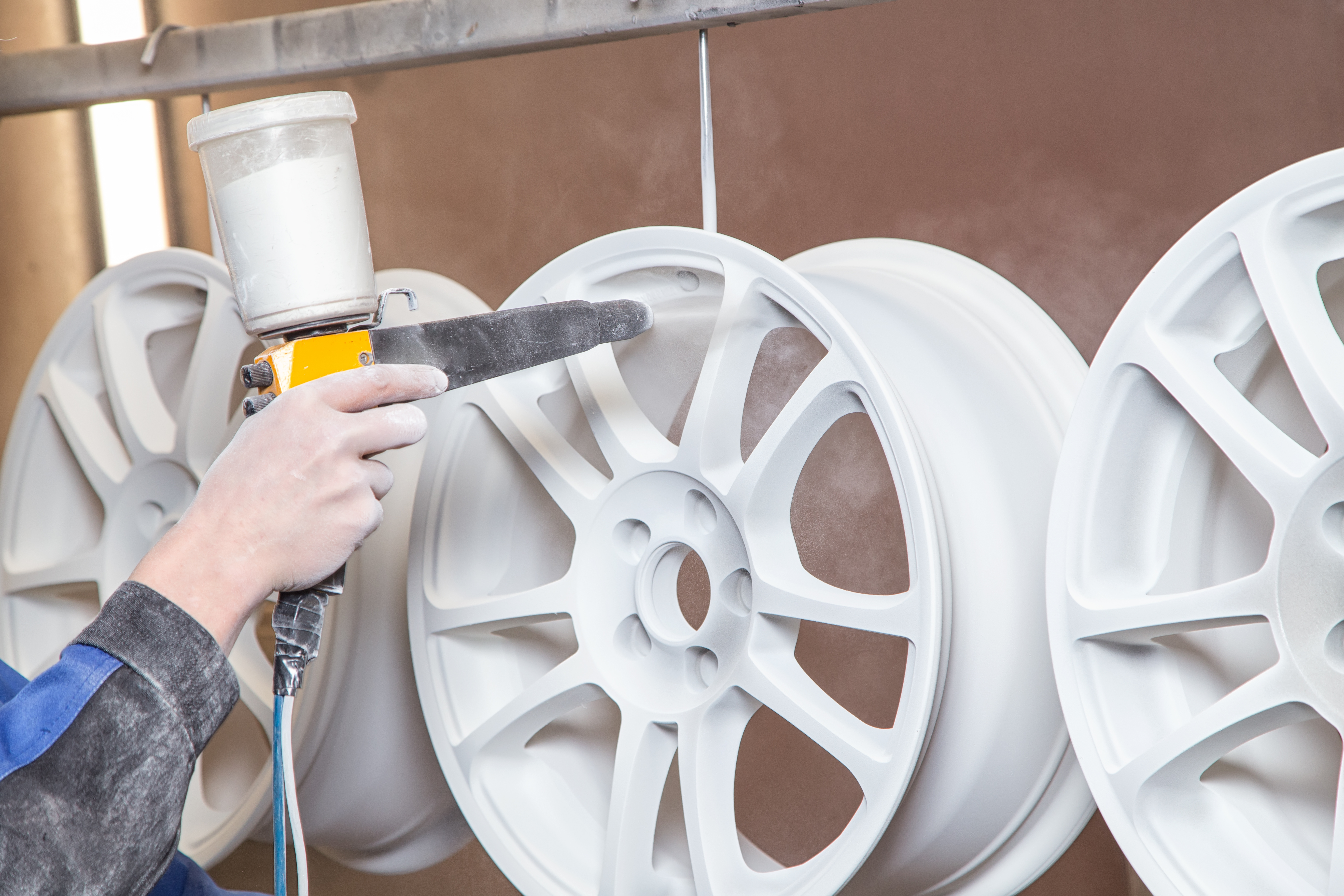
Painting of electroless nickel, mainly for aesthetic purposes, is common in certain industries. One such application is on plastic computer housings. In many cases, housings that have been electroless copper and EN plated for electromagnetic/radio-frequency interference (EMI/RFI) shielding are subsequently painted to improve the appearance of the housing and texture over any roughness. The plated housing is painted to match the color of the underlying plastic so any scratches that penetrate through the paint will not easily show up.
Painting can also be done to improve corrosion resistance of the coating system. The actual coating method used will depend upon the resin system of the paint.
Blackening
EN deposits are sometimes darkened for certain optical and aesthetic applications. This can be accomplished either through blackening of the EN deposit itself or by applying a black deposit on top of the EN deposit.
Blackening the EN deposit typically entails subjecting a mid-phosphorus deposit to a solution of nitric acid and etching the deposit to develop the black color. Mid-phosphorus EN deposits are used because they are attacked by acids and darken the most compared with other formulations. The dark color is the result of the formation of microscopic conical pits in the deposit, which trap incident light and prevent it from reflecting from the surface. Solar absorbances of 0.995 have been reported using this process. The resulting surface is only good for optical applications because the surface is very fragile and can be scratched and worn away easily.
Example formulations used for blackening EN deposits include:
- Nitric acid (HNO3) at concentration of 50 vol%, temperature of 50°C, and time of 15–20 sec
- Concentrated HNO3 saturated with nickel sulfate, 22°C, 20–30 sec.
For non-optical applications that require wear resistance, blackening is inconsistent and typically results in a mottled brown to black surface. For applications requiring a more functional, pleasing appearance, users can apply top coats such as electrolytic black nickel, electrolytic black chromium, or electrolytic blackenable alloys such as zinc/nickel.
Brazing
Several niche applications exist utilizing high-phosphorus electroless nickel as a brazing material to weld certain components together. In these applications, high-phosphorus (10–12% P) EN deposit is used to replace amorphous nickel-phosphorus braze alloy foil preforms (12–19% P). The EN plating helps avoid potential contamination from handling complex parts to attach the braze preforms, and also ensures that the braze alloy is properly located on a part.
RELATED CONTENT
-
Sizing Heating and Cooling Coils
Why is it important for you to know this?
-
Choosing and Troubleshooting Copper Electroplating Processes
Learn more on this inexpensive and highly efficient process.
-
Gold and Silver Plating Basics
An overview of precious metal electroplating processes.


