Stopping Bond Lift in Aluminum-to-Gold Wire Bonds
Critical plating configuration for reliable aluminum-to-gold wire bonds.
#pollutioncontrol #masking
In the world of high-reliability microelectronics—with aerospace, defense and medical implantation applications—devices are exposed to harsh environments and operated under extreme conditions.
More importantly, they cannot fail. If they do, chances are people die. So reliability is taken very seriously by device manufactures and their customers alike.
Featured Content
This manifests in the form of qualified materials, approved processes, certified manufacturing lines, specified test protocols, rigorous screening methods, standardized performance criteria, and so on.
But there are still so many ways to fail, and unfortunately new ways come along every day.
Microelectronic devices come in a variety of forms and functions: converters, regulators, amplifiers, modulators, receivers, transceivers, multiplexers, couplers, memory units and reference devices, to name a few. And they do everything from power management to line control, from data conversion to memory storage, from pulse modulation to signal amplification, from voltage regulation to EMI filtration.
Notwithstanding this diversity of functionality and componentry, there are just a few standard processes used in their assembly: die attach, wire bond and lid seal.
Carefully Regulate Process
Needless to say, manufacturers of high-reliability microelectronics develop considerable expertise, competency and skill within these core processes, and they carefully regulate process inputs and operational parameters.
Nowhere is this truer than in the domain of microelectronic devices that deals with power management and conversion. These devices compound the effects of harsh environments and extreme applications with some of their own: high heat generation, current density, and creative designs that stretch the limits of assembly processes and material properties alike.
Case in point: Most of the devices mentioned above use wire bonds with diameters in the 1-5 mil range, while power converters use bond wires with diameters as large as 20 mil. Many of the devices use the same metal for both wire bond and bonding substrate (or bond pad)—such as gold-on-gold or aluminum-on-aluminum; but power converters employ a mixed-metal design consisting of aluminum wires and gold bond pads.
These two distinctions—large diameter wires and mixed-metal designs—stretch the capability of the wire bonding process and increase the influence of the constituent materials’ properties on wire bond reliability.
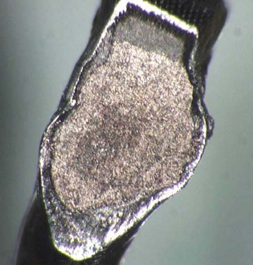
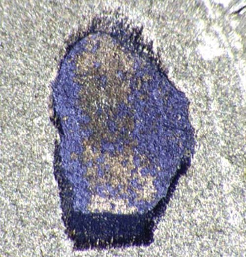
This investigation began as a root cause analysis into the infrequent, albeit potentially disastrous, separation of large diameter Al wires from Au-plated bond pads in microelectronic devices. Such an event is called a bond lift; it is a highly undesirable, general indication of a poorly performing wire bond process.
Well Examined
In this case, however, the wire bonding process had been thoroughly examined and vetted for optimization. The materials were also examined, both bond wire and the bonding substrates, and found to comply with all specifications and requirements. Their manufacturing processes were examined as well, and found to be in control and conforming to industry best practices. The root cause lay elsewhere.
Cross-sectional examination of the wire bond lift (the failure mode) showed that it always originated at one of two depths within the plating—at either the Au-Ni interface (nickel serves as an underplating for the gold), or mid-depth within the Au plating layer—with evidence of voiding frequently observed at the lift site. Focused ion beam (FIB) microscopy revealed the gold plating consisted of several layers of gold grains of varying size, although generally small, with no discernible epitaxy at the Au-Ni interface.
These revelations prompted examination of the gold plating process (electrolytic/rack) and the discovery that the standard operating procedure was to plate the gold in two stages to ensure the coverage of bare spots created by electrode contact points. The plating process consisted of a 5-8 µin gold strike followed by 30-50 µin of bulk Au, re-positioning of rack contact points to expose the bare spots for plating, and another 5-8 µin Au strike followed by a final 30-50 µin of bulk Au. A correlation was henceforth established: The depths of the failure mode origination sites (the Au-Ni interface or Au mid-depth) correlated perfectly with the strike/bulk, strike/bulk buildup of gold plating and the consequent multi-layer grain configuration.
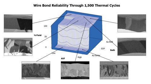
But was the grain structure causal to the bond lifts? To answer this question, an enhanced central composite design experiment was performed to relate wire bond reliability and gold plating microstructure. The experiment produced a broad spectrum of gold platings, 13 in all, using three plating bath combinations and five plating rates (drive currents). Each bath-rate permutation was plated to final thickness and incorporated in the assembly of functional devices, producing more than 1,800 Al-to-Au wire bonds. The assembled devices were screened, tested and processed through 1,500 -55°C -to- 150°C thermal cycles. Reliability was qualitatively defined as renitence to thermal cycling, quantitatively determined by the number of cycles without failure.
3 Points
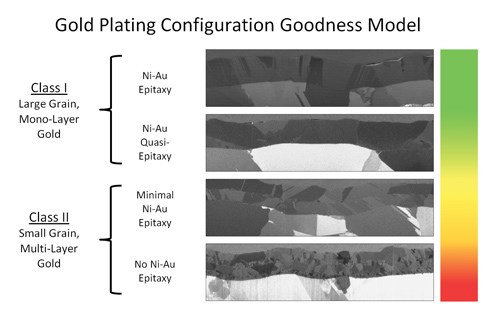
A response surface was generated from the experimental data, the examination of which is instructive on three cardinal points. First, the grain configuration of the gold plating is causal to the long-term reliability of Al-to-Au wire bonds. The SOP condition performed as expected with generally high reliability, while as yet producing the occasional, low-frequency bond lift. It presented a plating microstructure consisting of two or more distinct layers of gold. This result replicated production performance and validated the experiment’s control condition. Strike gold platings produced microstructures which consisted of small, randomly distributed gold grains with no evidence of layering or Ni-to-Au epitaxy. Wire bonds formed with these substrates failed at a catastrophic rate, with most failures occurring within the first 20 thermal cycles. Bulk gold platings presented large grain mono-layer microstructures, which produced very robust and reliable wire bonds. Permutations with this condition passed 1,500 thermal cycles without a single bond lift.
Second, the microstructure produced by the SOP gold strike is prohibitive to the formation of large grain, mono-layer gold. This point is clearly illustrated by the interruption of grain growth between the first and second bulk platings of the SOP condition and the complete absence of large grain microstructures within strike-only platings.
This effect is not unexpected since strike and bulk plating baths are designed to perform different, albeit complimentary, functions. A gold strike is used to initiate grain nucleation, which it does with both high efficiency and high frequency; bulk plating precipitates the growth of grains from the nucleation sites. Strike-only platings are formed through continued layering of nucleation sites and cannot, therefore, develop and grow large grain structures. They consist of small, under-developed grains that eventually become columnar in shape, and have a relatively large fraction (by volume) of interstitial space and grain surface area. These characteristics combine to make strike gold microstructures inherently more frangible and porous than their large grain counterparts. The latter characteristic, porosity—and resultant void aggregation—was a factor contributive to the root cause of the bond lift.
Third, excellent plating characteristics and robust wire bond performance were achieved without strike plating. Bulk/bulk permutations were plated with the following sequence: 30-50 µin of gold deposited directly on the Ni underplating, followed by a second 30-50 µin of gold deposited after contact point repositioning. These permutations consistently produced large grain, mono-layer gold plating that demonstrated excellent adhesion and wire bond reliability. This point begs the question: Is a gold strike really necessary?
Root Cause?
The root cause of the wire bond lifts was determined to be the prohibition of large-grain growth within the gold plating because of an excessive presence of strike gold. By reducing the amount of strike gold in the plating, its perturbative effects were retarded, and ultimately mitigated. So, for high reliability large diameter Al-to-Au wire bonds, gold plating processes must be optimized to produce large grain, mono-layer gold. The inherent conduciveness of this microstructural configuration to robust bonds is derived from its bedrock-like properties. It is a uniform, non-porous, and contiguous substrate of ultra-high purity. These properties make large grain, mono-layer gold the ideal substrate for any application requiring the bonding of aluminum wires.
Richard Share is principal at Share Consulting. His research is presented by permission of the Hi-Rel Division of International Rectifier Corp. He can be reached at share@sharellc.com.
RELATED CONTENT
-
Reducing Powder Coating Waste
Coating application is often overlooked as a potential money saver, but recognizing opportunities within this area is crucial to an efficient operation.
-
Plating Process Control
The cornerstone of quality and productivity for any finishing operation, process control is a plater’s key to success. To find out how far techniques have come, where they’re headed in the future, and how platers can raise the bar, Products Finishing convened a panel of experts for a roundtable discussion on the topic. With well over 100 years of combined plating experience, experts Greg Arneson, Art Kushner, Peter Gallerani and Joelie Zak share their thoughts.
-
Better Alloy Control of Alkaline Zinc Nickel Baths
The factors that influence nickel content in deposits from alkaline non-cyanide zinc nickel baths.


