AES Research Project #16: Final Report (1965) On the Mechanism of Metal Electrocrystallization
Under Research Project #16 of the American Electroplaters’ Society, the mechanism and kinetics of metal electrocrystallization were studied at the University of Pennsylvania from 1955 to 1965. What follows is the final summary paper of the project work. In these studies, electrochemical techniques are combined with the continuous observation in situ of the growing electrodeposit on various crystal planes of copper.
by
A. Damjanovic
Featured Content
The Electrochemistry Laboratory
University of Pennsylvania
Philadelphia, Pennsylvania, USA
Originally presented at the AES 52nd Annual Convention, New York, NY, July 12, 1965, and published as A. Damjanovic, Plating, 52 (10), 1017-1026 (1965)
Editor's Note: Under Research Project #16 of the American Electroplaters’ Society, the mechanism and kinetics of metal electrocrystallization were studied at the University of Pennsylvania from 1955 to 1965. What follows is the final summary paper of the project work. A printable version of this paper can be accessed HERE.
ABSTRACT
In these studies, electrochemical techniques are combined with the continuous observation in situ of the growing electrodeposit on various crystal planes of copper. Morphology of the deposit on various crystal planes is affected by current density and a small amount of surface-active agents. Growth of various types of deposit can be explained by simple mechanism of step propagation, the origin of the steps being either the initial misorientation of the substrate or the emerging screw dislocations. The change of electrode surface with time of the deposition is analyzed, and the effect of this change on the electrochemical behavior of the electrode and on the apparent exchange current density is discussed. Activity varies with crystal plane.
Under Project 16 of the American Electroplaters' Society, the mechanism of metal electrodeposition has been studied in the Electrochemistry Laboratory of the John Harrison Laboratory at the University of Pennsylvania since October 1955. This study grew from the consideration that, although considerable technologically important work had been done in the field of metal electrodeposition, and a number of papers had been published, there was a lack of knowledge of the fundamental, atomic mechanisms by which the process of metal electrodeposition occurs.
Much of the work on electrocrystallization at that time was confined to the morphological study of the deposit and to the determination of the conditions required for the formation of deposits with some particular properties. This aspect of metal deposition was far more advanced than our understanding of the processes themselves, of the "atomic" mechanisms which lead to the formation of a particular deposit, of the role and the importance of various factors which are known to affect the deposit, and of the kinetic analysis of the deposition process under given experimental conditions. It seemed reasonable to expect that the advance in technological electrodeposition would be speeded up if the elementary processes occurring during the deposition were more fully understood.
One reason for this lag in fundamental knowledge in comparison to the practical art of producing a desired type of electrodeposit is the complexity of the processes involved, particularly under practical conditions of electrocrystallization. To mention but two complicating factors: first, the role of surface-active agents, so widely used in practice, which may affect the mode of crystallization even in small concentrations; and, second, the inherent change of the electrode surface during growth, which may result in the change of mechanism, the rate of the reaction with time of deposition, or both. These changes, in a cycling process, may affect the growth itself.
For these reasons, and to simplify the interpretation of experimental results, in the first stage of the study of metal electrodeposition in this laboratory, experiments were carried out under conditions of "high purity" of solutions, and for lengths of time short enough to prevent any appreciable change in the electrode surface which results from growth during the measurements. The aim at this stage of study was to elucidate the path taken by a hydrated metal ion from a position in the solution until it reaches a growth site on the electrode and becomes incorporated into the crystal lattice of the metal. This short time study has provided basic knowledge concerning the reaction path of a metal ion, and the reaction step in it that proceeds with the highest resistance and hence controls the rate of the overall reaction.
After this study had been successfully completed, a logical next step was to extend the study to long time deposition or, in other words, to electrocrystallization itself. Again, this work has been carried out under controlled conditions of solution purity.
Progress made during the first stage of the study on electrodeposition has been reported at previous meetings1,2 of the Society. Here, the main results obtained during that period of the study are briefly reviewed, and progress made in the study of electrocrystallization is described. Electrocrystallization of copper was studied, under Project 16 of the American Electroplaters' Society, on the three main planes of copper single crystals.
Paths taken by an ion in electrodeposition
The first problem in the study of metal electrodeposition is to determine the path taken by a hydrated ion in the solution until it becomes incorporated into the lattice of the metal. A hydrated cation in the outer Helmholtz plane has to cross the double layer and to dehydrate before it becomes incorporated into the metal lattice. A theoretical analysis by Conway and Bockris3,4 showed that when an ion undergoes charge transfer, this dehydration process should proceed in stages, like most other chemical or electrochemical reactions, rather than in one single reaction step. In the simple case of a monovalent cation, a hydrated ion first loses one part of the H2O molecules in its hydration shell and becomes attached to the electrode surface. Such a partially dehydrated metal ion* on the electrode surface is called an adion (Fig. 1).
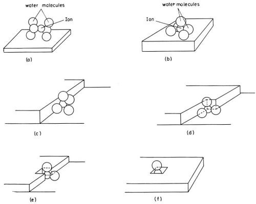
Figure 1 - An ion in the process of deposition dehydrates in stages. Possible modes of hydration of an ion at various sites on the electrode surface are illustrated.1-4,11
Adions form at any point on the electrode surface where ions can be discharged. On the surface, an adion, as an adsorbed species and not yet a part of the metal lattice, is mobile; it randomly migrates along the electrode surface and around adsorbed molecules of H2O until it reaches a growth site where it becomes further dehydrated and, finally, incorporated into the metal lattice. Figure 1 pictures a hydrated ion in the solution, an adion on the "flat surface" and an adion at various growth sites. A growth site, in an ideal case, is a kink in a microstep one atom high (Fig. 2). These microsteps on the electrode surface are called monatomic steps. An adion which diffuses to such a monatomic step is not yet to be considered as incorporated into the lattice of the metal. At the step it becomes further dehydrated and diffuses now along the step to a kink site in the step where it finally becomes incorporated into the metal lattice. At the kink site, an ion, not an adion any longer, is in contact with half of the number of atom neighbors it would have inside the metal, for which reason an ion in the kink site is said to be in the half crystal position.
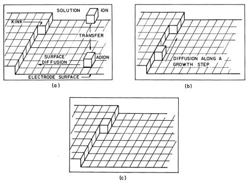
Figure 2 - Illustration of a path taken up by a metal ion in the process of deposition; (a): Transfer of the ion from the solution to a site on the metal surface and the diffusion of such an adion along the surface to a growth step; (b): diffusion of the ion along the growth step; (c): incorporation of the ion into a kink site.
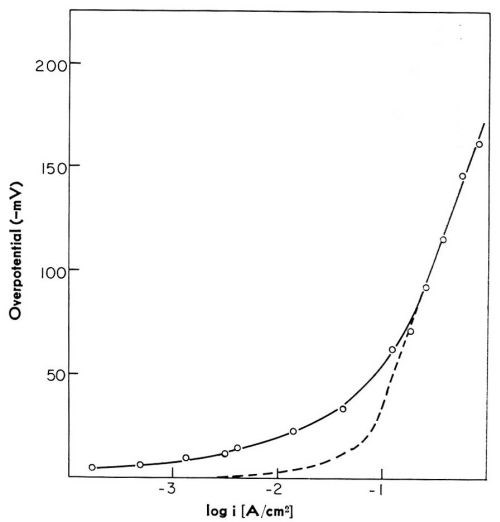
In this model of the reaction path, two partial processes are distinct - the charge transfer across the double layer with the formation of adions, and the surface diffusion of adions from sites at which cations have landed to monatomic steps. Each of these partial processes, or reaction steps as they are usually called, may control the overall rate of the reaction at a given electrode potential. Which of these reaction steps controls the rate of the reaction depends on the conditions of electrodeposition. Theoretical analysis predicted3,4 that at low cathodic overpotentials, surface diffusion of adions was likely to control the overall rate of the deposition; but, with increasing current density, and hence with increased over-potential, charge transfer should become the rate-controlling. This was subsequently confirmed by experiments with silver,6,7 copper8,9 and with solid and liquid gallium10,11 electrodes. At higher current densities, a linear potential-log current density relation was obtained. This is illustrated in Fig. 3, for the case of copper. The linear relationship which is observed is characteristic of charge transfer being controlling. At low current densities, the relationship deviated from linearity, and for the same current density the overpotential is higher than if charge transfer were the rate-controlling reaction step. This deviation was in accord with the surface diffusion of adions being rate-controlling at low overpotentials. The charge transfer was, however, the rate-controlling step on liquid gallium electrodes even at low current densities; on solid gallium electrodes, surface diffusion of adions controlled the rate of the reaction only at low overpotentials. Of course, on a liquid electrode, each site on the surface is a growth site and no surface diffusion of adions is required even at low overpotentials. With these experiments, therefore, the predicted path via surface diffusion was confirmed.
Direct deposition at kink sites
The direct transfer of ions from the solution to growth sites, where they become incorporated into the metal lattice, could be an alternative path to the proposed model of the charge transfer at any point on the electrode surface and subsequent surface migration of adions to a monatomic step. Theoretical analysis3,4 showed, however, that the activation energy for the direct transfer to a growth site would be prohibitively large since an ion has to dehydrate, not gradually, but in one step. Were the ions to deposit directly at the steps on the electrode surface, a liquid electrode, with no restriction in respect to sites at which this deposition can occur, would be far more active than a solid electrode both at low and at higher current densities. This is contrary to experimental observation on liquid and solid gallium electrodes.
Monatomic steps on an electrode surface
The models described for the reaction paths taken by an ion from the solution to a growth site, require presence of monatomic steps on an electrode surface, or on each face of a small, single crystal which constitutes a grain of a (polycrystalline) electrode. In Fig. 4, a ping-pong ball model of a surface with a monatomic step on it is shown. An ideal monatomic step will, however, during the deposition receive the deposited ions and will soon grow laterally out of the surface and leave the surface without steps. Hence, a mechanism has to exist which creates and maintains monatomic steps on the surface.
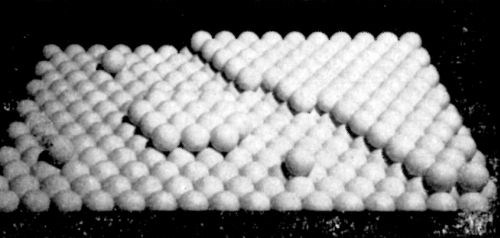
Figure 4 - A model of a surface with a "monatomic" growth step. A nucleus on the flat surface may create some of these growth steps.
One origin of these steps may be found in two-dimensional nucleation. Adions cluster on the surface and form an "embryo" (Fig. 4). The embryo is not, however, stable, and adions may leave it. It may become a stable nucleus and grow if additional adions join the embryo before it "decomposes." Analysis shows that the size of these embryos, and the number of them per unit area, depend critically on the overpotential.12 Only at higher overpotentials is the probability of the formation of nuclei sufficiently high and, consequently, sufficient density of monatomic steps is created. This can be illustrated by an experiment of Vermilyea13 on copper whiskers. Whiskers approach the ideal case of a single crystal with smooth side faces and practically no monatomic steps on them. If such a whisker is immersed into a CuSO4 solution and is polarized cathodically, no crystal growth occurs on the side faces of the whiskers until the overpotentials are sufficiently high (on perfect whiskers it is over 100 mv), that is, until nucleation becomes possible.** Copper, however, can be electrodeposited on most of the electrodes at overpotentials far below that required to start crystallization on whiskers. This shows that under such conditions, no nucleation is required to continue metal deposition.
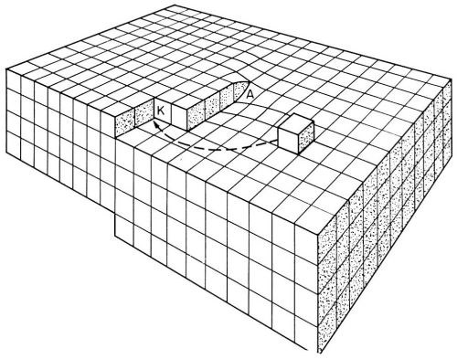
Figure 5 - Model of a surface with a screw dislocation emerging at A. At a point where the dislocation emerges, a step originates. These steps are suitable for growth by incorporation of adions. K is a kink site.
According to Burton, Cabrera and Franck,14 who analyzed crystal growth from the vapor phase, self-perpetuating monatomic steps are present on the growing surface. Such steps do not grow out of the surface as they receive deposited ions. These growth steps originate at points where screw dislocations emerge on the surface (Fig. 5). Incorporation of atoms at such a step will make the step advance. However, the step is fixed at the point where it originates (point of emerging screw dislocation). Consequently, it rotates around the emerging dislocation, and, in this process, does not grow out of the surface. Under favorable conditions, a step, instead of rotating as a straight unit around the emerging dislocation, may wind itself up into a spiral which eventually, with further growth, rotates as a whole around the dislocation (Fig. 6).
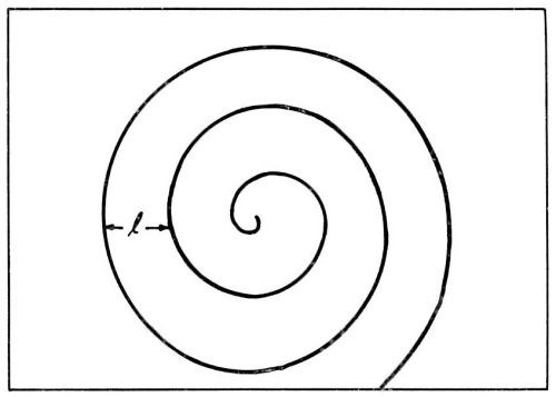
Figure 6 - During growth, a step originating at an emerging screw dislocation winds itself up into a spiral.
Similar growth mechanism should be applicable to electrocrystallization. The more growth steps due to screw dislocations are present on an electrode surface, the more easily will adions reach them and become incorporated into the metal lattice, and the surface diffusion of adions may cease to be the rate-controlling reaction step in the overall reaction. In fact, on heavily damaged crystals, with a high density of dislocations and, hence, of monatomic steps, surface diffusion of adions would not be expected to be a hindering factor in the overall rate of the reaction.
During the growth, the total length of monatomic steps (per unit surface area of the electrode) may increase with time. Consequently, the kinetics and the mechanism of deposition (or of dissolution) can change with time of deposition. This is particularly true in the early stage of deposition (or of dissolution) when initially straight monatomic steps first start to wind themselves up (into spirals) and increase the total length of growth steps.
It follows from this analysis that the screw dislocation mechanism can provide monatomic steps required to sustain the growth, and that there is no need for two-dimensional nucleation to occur.
Transient technique in the study of metal electrodeposition
The technique of short time pulses of constant current was used in the first stage of the study mainly for two reasons. First, in metal electrodeposition (or in dissolution) the amount of metal ions incorporated into (or leaving) the metal lattice, is less than that equivalent to a monolayer. Hence, the electrode surface does not change during the pulse and measurement. No significant movement of monatomic growth steps occurs, and the total length of these steps, and hence the number of growth sites per unit area, does not change appreciably. For this reason, a short time transient study is also called the "monolayer" deposition study.
The second reason for this choice of transient technique is that the potential-time transients at constant current density are characteristic of a given rate-controlling reaction step. The analysis of these transients on copper,9 silver,6,7 and solid gallium10 electrodes also confirmed that, at low current densities, diffusion of adions over the electrode surface is the reaction step which controls the overall rate of the reaction. At higher current densities, charge transfer is rate-controlling.
Electrocrystallization
Electrocrystallization is another aspect in the study of metal deposition, which follows monolayer deposition, and concerns itself with the processes occurring after the monolayer deposition was completed. The objective is to analyze the mechanism of the crystal growth on an atomic scale and to determine what are the factors affecting the kind of crystal form that will develop and, eventually, what are the properties of the electrodeposits.
Mechanisms and the rates of electrocrystallization on various crystal surfaces of a (small) single crystal composing a polycrystalline electrode may differ from one surface to another. Thus, the rate and the mechanism on the (111) crystal plane can be different from that on the (110) plane. It is advantageous, therefore, to study electrocrystallization first on each of the main crystal planes separately, and then to approach the more complex problem of the electrocrystallization of polycrystalline deposits. In our laboratory, this line of approach was taken and electrocrystallization of copper onto copper single crystal faces parallel to either the (111), (110) or (100) crystal planes was studied. In Fig. 7, the atomic structures of these crystal planes are illustrated.
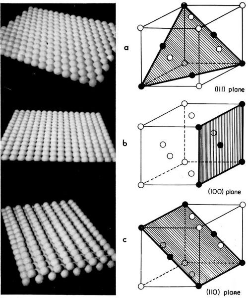
Figure 7 - Models for main crystal planes of a copper single crystal. (a): (111); (b): (100); (c): (110) plane.
To study metal crystal growth, electrochemical measurements alone are not sufficient, as the growth, and the change of the surface with the growth, are not reflected in a simple way from the data of electrochemical measurements. Ideally, one would wish to know for each crystal face, or crystal surface, all structural data, which arise from the growth, on the finest scale at all times of deposition. Hence, continuous observation of the growing electrode surface is required.
There is still another requirement. In order to avoid the complicating influence of surface-active agents on electrocrystallization, which are mostly organic and probably always present in solutions if they are not purified, deposition should be carried out from a solution of known high purity. This simplifies the interpretation of the results.
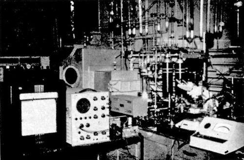
Figure 8 - A photograph of the experimental set-up for the study of electrocrystallization.
These two requirements involve highly elaborate experimental technique. This is illustrated by a photograph showing the experimental set-up satisfying both requirements (Fig. 8). A light microscope was used for continuous observation. In order to maintain high purity of the solution, the objective of the microscope was not immersed in the solution. Also, the solution and the electrode surface must not be in contact with the atmosphere. To satisfy these requirements, an all-Teflon cell was constructed15 (Fig. 9). It enables continuous, in situ, observation and microphotography of the growing deposit to be made with a relatively high useful magnification of 600 to 800 X. Another advantage of the in situ observation is that the rates of growth of individual growth forms are obtained.
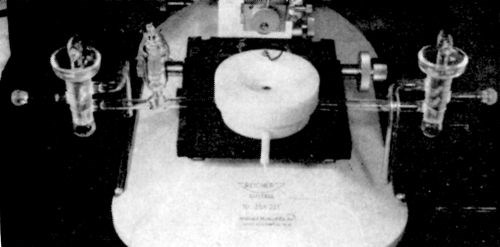
Figure 9 - A Teflon cell for continuous, in situ observation of the growing electrodeposits.
Deposition was carried out at constant current densities from 1 to 50 mA/cm2, until the average thickness of the electrodeposit corresponding to about 10 coulomb/cm2*** was reached. Photographs (through the solution and the cover glass) have been taken at regular intervals of time. The types of deposit formed are characteristic of the initial substrate orientation, but depend also on other factors, such as purity of the solution, presence of surface-active agents in the solution, current density and temperature. In the following, a description of some types of deposit on the three main crystal planes of copper is given.
Copper electrodeposits on single crystal faces of copper
Characteristic types of growth forms observed16-18 are shown in Fig. 10 for (100) and in Fig. 11 for (111) and (110) planes. They are pyramids, blocks, macrosteps and ridges. In Table 1, data on the forms of deposits which grow at a given current density on (100) plane are summarized.16 These growth forms also have been observed by other authors.19-22 Pyramidal growth usually occurs at low (<10-15 mA/cm2) current densities, and blocks at somewhat higher (>10-15 mA/cm2) current densities than that at which pyramids form. Purity of the solution is an important factor here. If a surface active agent is present in the solution, the range of current densities at which pyramids form decreases, and blocks appear at lower current densities than from a solution without the surface active agent.16-18 If the concentration of a surface active agent increases above a certain level, none of these growth forms develop, but a ridge type of growth appears. Thus, in copper deposition onto the (100) plane of a copper single crystal, a concentration of n-decylamine of 10-7M/L was sufficient to suppress completely the formation of pyramids, or of blocks and cubic layers, and only a ridge type of deposit formed.16
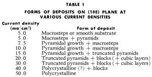
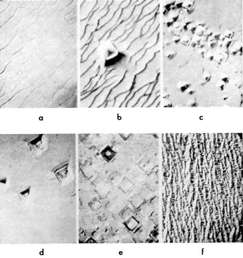
Figure 10 - Growth forms on the (100) plane of a copper single crystal: (a): macrosteps (5 mA/cm2); (b): macrosteps + occasional pyramids (5 mA/cm2); (c) and (d): pyramid formations (5 mA/cm2); (e): block form of growth (15 mA/cm2) and (f): ridge form of growth (10 mA/cm2).
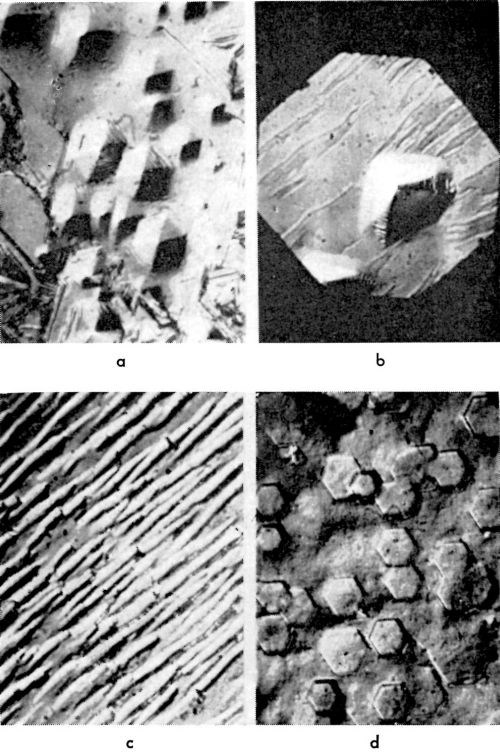
Figure 11 - Growth forms on the (111) and (110) planes of copper single crystals: (a) and (b): pyramid forms on (111) plane (5 mA/cm2); (c): ridge form of growth on (110) plane (10 mA/cm2) and (d): block form of growth on (111) plane (5 mA/cm2).
Macrostep formation and propagation
Below about 5 mA/cm2, relatively smooth deposits or deposits with some macrosteps on the surface form. Pyramids grow only occasionally. These macrosteps appear also at higher current densities but together with pyramids.
Initially, the density of these macrosteps is high, but with time of deposition, the average distance between these macro-steps increases. At the same time, the heights of the macrosteps also increase. The average distance between macrosteps and the average heights of macrosteps increase linearly with the time of deposition (Fig. 12). The ratio of the average height and the average distance remains independent of the time of deposition.† It was observed also that in a given experiment, these macrosteps all propagate in one direction. The above two facts are consistent with the hypothesis that the origin of macrosteps lies in the microsteps, ideally monatomic, which arise from the misorientation of the original substrate with respect to the "perfect" orientation in which the exposed surface would be exactly parallel to the (100) crystal plane. A misorientation of only a fraction of a degree would result in a high density of monatomic steps. During deposition, monatomic steps will receive atoms and thus propagate. Some monatomic steps would propagate faster than others and catch up with the preceding steps to form clusters of monatomic steps, and eventually visible macrosteps. This is illustrated in Fig. 13.
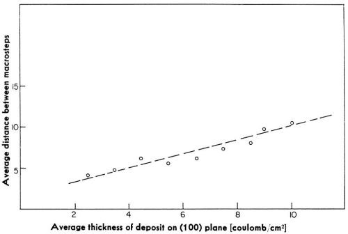
Figure 12 - Dependence of the average distance between macrosteps on the average thickness of the deposit.
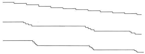
Figure 13 - Schematic representation of a macrostep composed of a number of small (monatomic) steps.
To check the hypothesis, a single crystal of copper was repolished in such a way that the misorientation, defined by the angle which the true surface makes with the (100) crystal plane, also changes.16 From the heights and density of macrosteps, it was concluded that the original misorientation is approximately equal to 0.3°. The crystal was repolished so as to change the orientation by about one degree but in the opposite direction. In subsequent experiments, macrosteps indeed propagated during growth in a direction opposite to that prevailing before repolishing. Hence, these macrosteps are formed from microsteps originating in misorientation of the initial substrate with respect to the ideal surface orientation.
Once these microsteps had formed, further increase in their height and in the distances between them does not necessarily occur by a mechanism in which one macrostep travels faster and catches the other. Rather, the increase occurs by fading of some of the macrosteps. In Fig. 14, three photographs of the same surface area show a macrostep disappear by fading away starting from one end.16 This is schematically illustrated in Fig. 15. The macrostep in the middle fades away by decomposing itself into smaller, and eventually invisible microsteps, ideally into monatomic steps.
.jpg;maxWidth=600)
Figure 14 - In situ photographs of the same area of a copper electrodeposit on the (100) plane. A step (at x) is fading out from one end. Average thicknesses of the deposit a: 8.5, b: 9; and c: 9.5 coulomb/cm2.
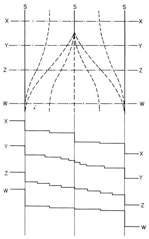
Figure 15 - A model for the fading out of macrosteps. Macrostep at the top middle fades out. X, Y, Z, W, are cross sections.
Rate of microstep propagation
Macrosteps propagate over the surface with an average rate which is proportional to the given current density.16,17††
Knowing the rate, v, of macrostep propagation, the average height, h, and the average density of macrosteps, it is possible to calculate the average rate of copper deposition at these macrosteps. It is equal to:
istep=z∙F∙(h/l)∙v∙g∙1/M (1)
where z is the valency, F is the Faraday constant, l is the average distance between macrosteps, g is the specific and M the atomic weight of the metal. It was shown16,18 that only a few per cent of the total deposited metal atoms incorporate into the metal lattice at these macrosteps. This was unexpected, and a mechanism had to be found to account for most of the deposited atoms. Where and how do atoms incorporate into the metal lattice? Occasional pyramids could account for less than one per cent of the deposited metal. The only explanation was that adions must incorporate into the lattice on the apparently "smooth" substrate between macrosteps.
The incorporation on a "flat" substrate may occur by one of the following mechanisms:
(i) On the "smooth" portion of the electrode surface between macrosteps, two-dimensional nuclei form and provide monatomic steps suitable for growth. This mechanism is improbable since high overpotentials are required for the formation of stable nuclei, as discussed above;
(ii) Monatomic steps are created by the self-perpetuating screw dislocation mechanism and
(iii) Monatomic steps may be formed at the bottom of a macrostep by incorporation of adions at its bottom. Mechanisms (ii) and (iii) are equally possible.
Mechanism of pyramid formation
The growth of pyramids can be explained by successive nucleation and growth of atomic monolayers one over another. A formed layer has already propagated a certain distance before a new layer is nucleated on top of it.††† This mechanism is improbable since high overpotentials would be required for the nucleation. Alternatively, the mechanism of the growth of pyramids may involve a screw dislocation. In Fig. 16, this mechanism is illustrated with the aid of a model. The step emerging at the dislocation winds itself up and around the dislocation, producing a cone-like body. Due to the crystal symmetry, instead of the cone, a rectangular pyramid forms. On the (100) plane, these are fourfold (Fig. 10), and on the (111), they are either triangular or hexagonal (Fig. 11).
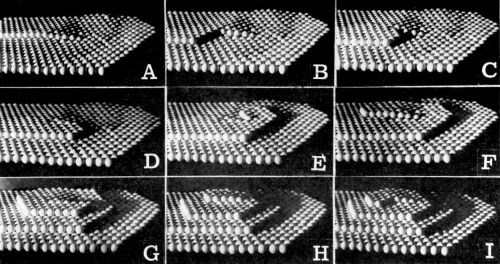
Figure 16 - A model of pyramid formation with a screw dislocation.
On the apex of the pyramid, there is an emerging screw dislocation (or group of dislocations) which operates and sends out closely spaced monatomic steps. If, for any reason, this dislocation stops operating and sending out monatomic steps, the pyramid truncates. In Fig. 17, such truncated pyramids are shown. As the side faces of a truncated pyramid continue to grow, the truncated pyramid transforms into a block, and eventually into a (large) cubic or hexagonal layer.‡
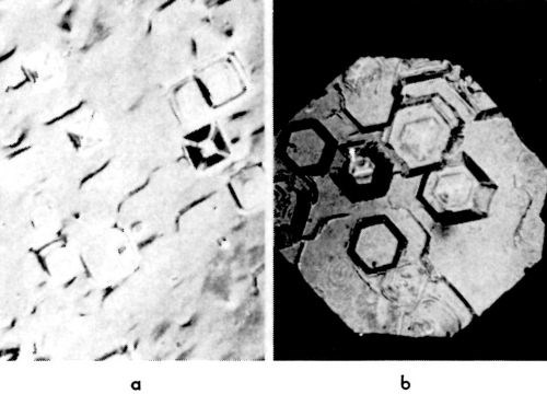
Figure 17 - Truncated pyramids: (a): (100) plane, 10 mA/cm2; (b) (111) plane, 10 mA/cm2.
Now, it can be asked, under what conditions does this truncation of pyramids occur? They tend to truncate more frequently at higher current densities, and also in the presence of some surface active agents. Thus, in the presence of n-decylamine (~10-8-10-9 M/L), truncation on the (100) plane occurs at an early stage of deposition while, without n-decylamine, truncation under the same condition is rare.16 It is postulated that the emerging screw dislocation may become blocked by adsorbed "impurities." This would make the dislocation inactive and cause truncation. The side faces of a (truncated) pyramid, whose apex is blocked by "impurities," are still active and continue to grow.
Hence, the same mechanism accounts for the formation of pyramid, block and layer type of structures.
Summary of the mechanisms of growth
Finally, it should be noted that a monatomic step originating at an emerging screw dislocation will not wind itself up into a microspiral which may lead to the formation of a pyramid,‡‡ unless a critical overpotential is reached. For copper deposition on a (100) plane, it appears that this critical potential is around 20 mV, since at current densities below about 5 mA/cm2, no pyramids grow (or rarely) and either smooth deposits or deposits containing macrosteps develop. At higher current densities (5-30 mA/cm2), the screw dislocation mechanism of growth operates and pyramids form on a smooth substrate, or on a substrate with macrosteps originating from misorientation. Pyramids, however, will soon truncate at high current densities and transform into blocks. Eventually, at current densities above about 30 mA/cm2, numerous outgrowths form, and the deposit resembles a polycrystalline aggregate.
Growth on the (111) and (100) planes can be accounted for by the same mechanisms. A (111) plane is, however, less sensitive to surface active agents than is the (100) plane. Still, truncation of pyramids on the (111) plane readily occurs in the presence of n-decylamine. A (110) plane behaves differently from the other two. Though macrosteps and occasionally (tetragonal) pyramids do form, they are rare, and a ridge type of deposit readily appears. This would indicate that the (110) plane is far more affected by surface active agents than (100) or (111) planes. This is probably due to much stronger adsorption bonds on the (110) plane than on the other two planes. No mechanism for ridge formation has been suggested.
Change of electrode potential with time of deposition
At any given current density, the potential changes with the time of deposition, particularly during initial stages of deposition. In Fig. 18, overpotentials are plotted versus aver age thickness of the deposit for deposition at 5 mA/cm2 on the three crystal planes. The largest change in the potential among these three planes occurs on the (111) plane. The overpotential on this plane decreases with increasing thickness of the deposit.‡‡‡ In contrast to this, on the (100) plane, the overpotential increases with the average thickness of the deposit.‡‡‡ The magnitude of the increase is, however, far less than the corresponding decrease on the (111) plane. On the (110) plane, the change in the potential is the least of all of the three planes. Reasonably steady state is established on the (111) plane at an average thickness of the deposit corresponding to about 6 coulomb/cm2◊. On the (100) plane, steady state is established at about 2-4 coulomb/cm2,◊ and on the (110) plane even earlier.
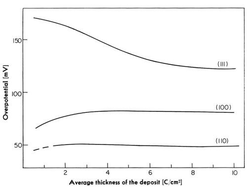
Figure 18 - Change of electrode potential with average thickness of the deposit at 5 mA/cm2.
The observed decrease in the potential on the (111) plane could be accounted for if the surface area of the crystal increased with the time of deposition by about 400 percent. Calculations show that the roughness of the electrode, due to macrostep formation and to the growth of pyramids, can account for no more than about a 20 percent decrease in the overpotential. On the (100) plane, where the overpotential increases with average thickness of the deposit, the electrode surface would have to be diminished by about 20 to 30 percent. Therefore, some other explanation has to be found for the observed overpotential changes since the change in the roughness of the electrode surface alone is not sufficient. A more likely explanation is given below.
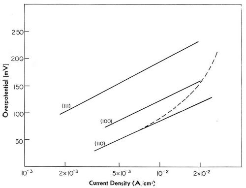
Figure 19 - Electrode potential-log current density relationship for main crystal planes.
Mechanism of the reaction
When overpotentials are plotted versus log i, reasonably linear relations are obtained for each crystal plane, type of deposit, and average thickness of the deposit.18 For the same crystal plane, Tafel lines obtained at an early stage of deposition and that obtained at a final stage show a relative shift with respect to each other. Tafel slope, however, is the same in both instances.
In Fig. 19, Tafel lines for all three crystal planes, and for initial and final stages of deposition, are given. All of these lines have the same Tafel slope close to 2RT/F. This slope is characteristic of the charge transfer of the first electron being the rate-controlling reaction step according to:
Cu++aq + e– ⇒ Cu+aq slow (2)
Cu+aq + e– ⇔ Cuad fast (3)
It has already been observed by Bockris and Kita9 that only on electrodeposited electrodes first charge transfer, and not surface diffusion of adions, is rate-controlling at all current densities. In contrast to this, on annealed electrodes, surface diffusion is the rate-controlling reaction step at low current densities. In these experiments on electrocrystallization, it is shown that the first charge transfer is the rate-controlling reaction step for all three examined crystal planes and at all current densities.
Exchange current densities
The following generalizations can now be made from the current-potential relationships.
1. Current densities corresponding to a given crystal plane during the initial stages of deposition are in the order:
i111 < i100 < i110 (4)
Current density, or activity, is lowest on the most closely packed (111) plane, and highest on the least closely packed (110) plane (see Fig. 7). Since the reversible potential is (approximately) the same for all planes,23 extrapolation of current densities towards zero overpotential would give the "exchange current densities," i°'s, in the same order. The ratio of i°110/i°111 is about 10.
2. Since the same Tafel relationships were observed at the initial and final stages of deposition, the change of the overpotential with time cannot be explained in terms of changes in the reaction mechanism. The variation of the overpotential with time of deposition at a constant current density must then arise from a corresponding variation in the "exchange current densities." It is hypothesized that the latter change is due to the formation and growth over the initial substrate of new crystal faces of different activities.
Suppose, for instance, that an ideal (111) plane is initially exposed to the solution. It has an exchange current density corresponding to this plane, namely i°111, During the deposition, new growth forms develop, such as pyramids with their pyramidal faces, or macrosteps with their side faces. These new faces are of different crystal orientation, and most probably correspond to some higher indexed, less closely packed and thus more active planes, than the initial (111) plane, which is the least active. Hence, the initial (111) plane with low exchange current density is gradually replaced by some other planes with higher exchange current densities.
Suppose that on a surface parallel to (111) plane new faces form during growth. The total current density is then given by:
i = [(1 - A) i°111 + A i°hkl] • e-αFη/RT, (5)
where i°hkl is the exchange current density of the newly formed face with a fractional area A. If
i°hkl ≥ 10 i°111 (6)
(4) can be approximated to
i = (i°111 + A i°hkl) • e-αFη/RT. (7)
The area A will change with time. An increase in A by say 0.2 would be sufficient to explain the observed decrease in the potential on a (111) plane. Thus, instead of assuming a change in the surface area due to roughening of the electrode surface by a factor 2 or 4, the apparent exchange current density
(i°Ap)t = i°111 + At i°hkl (8)
increases with time by that factor. The subscript t indicates this time dependence.
In general, the apparent exchange current density will be the sum (over all the planes) of the products of the corresponding exchange current densities and the fractional area (Ahkl)t :
(i°Ap)t = ∑hkl i°hkl (Ahkl)t (9)
This equation24 holds for polycrystalline aggregates also, independently of whether short or long time polarization is considered, and accounts for the average nature of the electrochemical measurements. It holds, however, only if the mechanism and the rate-controlling reaction step is the same◊◊ on all crystal surfaces of a polycrystalline aggregate, or on all faces of a crystal exposed to the solution.
Changes in the overpotential with time during the deposition on a (100) plane are far less than those on a (111) plane. It is possible that on an initial (100) plane, growth forms develop both with the (111) and the (110) planes, that is with planes of both lower and higher activity, and the net result is a decrease in the overall activity. On the most active (110) plane, changes in overpotential are insignificant except at higher current densities and longer times of deposition where a ridge type of deposit forms. The side faces of the ridges most probably correspond to planes of much lower activity than is the (110) plane, and the overpotential for the same current density increases.18
Conclusion
The aim of this paper was to describe the work and to summarize the main achievements and results which have been obtained in the study of the mechanism and kinetics of metal electrodeposition under Project 16 of the American Electroplaters' Society.
Using short time transients, it was concluded that, in a simple metal electrodeposition, the reaction path is via charge transfer, diffusion of adions over the electrode surface and incorporation of adions into the lattice. Which of these individual reaction steps is rate-controlling depends on the experimental conditions. In the monolayer deposition study, at low current densities, surface diffusion usually controls the overall rate of the deposition. At high current densities, charge transfer becomes rate-controlling.
In the study of electrocrystallization, or long time deposition, it was shown that the exchange current density depends on the crystal plane. It is higher on the loosely packed (110) plane than on the densely packed (111) plane. The long-known fact that during constant current electrodeposition, the potential changes with time, particularly during the initial stages of deposition, has been rationally explained by the change in the morphology of the deposit and the formation of new crystal faces with different activity.
Another aim of this paper is to show the importance of studying metal electrodeposition under conditions such that one has a well-defined electrode surface at any instant of deposition time. In the electrocrystallization studies, electrochemical measurements must be supplemented by parallel or simultaneous morphological observations. When these two techniques are combined, a more thorough knowledge of electrocrystallization processes on an atomic or molecular scale can be expected.
Once the basic mechanisms of electrocrystallization on individual crystal planes are well understood, the problem of initiation and growth of polycrystalline aggregates may be treated on a more mechanistic basis.
The importance of all these studies lies in the belief that once the basic principles of metal electrocrystallization are well known under the ideal experimental conditions, a more successful approach can be made towards better understanding of the more complicated but technologically very important processes of metal deposition in the field of electroplating, electroforming, electrometallurgy, and even of "electroless" deposition from solution or vapors.
Acknowledgement
I wish to thank Dr. J. O'M. Bockris, Mr. E.R. Bowerman, Dr. O. Kardos, Dr. J. Kruger, Dr. J.V. Petrocelli, Mr. G. Razumney, Dr. D.R. Turner and Dr. R. Weil for the criticisms they offered in the course of preparation of this paper.
References
1. B.E. Conway and J. O'M. Bockris, Plating, 46, 371 (1959).
2. J. O'M. Bockris, Proc. Amer. Electroplaters' Soc., 49, 17 (1962).
3. B.E. Conway and J. O'M. Bockris, Proc. Roy. Soc., 248, 394 (1958).
4. B.E. Conway and J. O'M. Bockris, Electrochim. Acta, 3, 340 (1960).
5. H. Gerischer, Z. Elektrochem., 62, 256 (1958).
6. W. Mehl and J. O'M. Bockris, Can. J. Chem., 37, 190 (1959).
7. A.R. Despic and J. O'M. Bockris, J. Chem. Phys., 32, 389 (1960) .
8. J. O'M. Bockris and M. Enyo, Trans. Faraday Soc., 38, 1187 (1962).
9. J. O'M. Bockris and H. Kita, J. Electrochem. Soc., 109, 928 (1962).
10. J. O'M. Bockris and M. Enyo, J. Electrochem. Soc., 109, 48 (1962).
11. J. O'M. Bockris and A. Damjanovic, in Modern Aspects, 3, Butterworths, 1964.
12. A. Damjanovic and J. O'M. Bockris, J. Electrochem. Soc., 110, 1035 (1963).
13. D.A. Vermilyea, J. Chem. Phys., 27, 814 (1957).
14. W.K. Burton, K. Cabrera, and F.C. Franck, Proc. Roy. Soc., 243, 299 (1951).
15. A. Damjanovic, M. Paunovic and J. O'M. Bockris, Plating, 50, 735 (1963).
16. A. Damjanovic, M. Paunovic and J. O'M. Bockris, J. Electroanal. Chem., 9, 93 (1965).
17. A. Damjanovic, M. Paunovic and J. O'M. Bockris, Electrochim. Acta, 10, 111 (1965).
18. A. Damjanovic, T.H.V. Setty and J. O'M. Bockris, to be published.
19. H. Seiter and H. Fischer, Z. Elektrochem., 63, 249 (1959).
20. H. Seiter, H. Fischer and L. Albert, Electrochim. Acta, 2, 167 (1960).
21. D.R. Turner and G.R. Johnson, J. Electrochem. Soc., 109, 778 (1962).
22. H.J. Pick, G.G. Storey, and T.B. Vaughan, Electrochim. Acta, 2, 196 (1960).
23. L.H. Jenkins and V. Bertocci, J. Electrochem. Soc., 112, 517 (1965).
24. A. Damjanovic, M. Paunovic, T.H.V. Setty and J. O'M. Bockris, to be published.
About the author (written in 1965)

Dr. Aleksandar Damjanovic was born in Yugoslavia on May 6, 1923. He studied chemical engineering at the Faculty of Technology, Belgrade, and in 1952, he received the degree in chemical engineering. From 1953 to 1957, he studied physical metallurgy and crystallography in Birmingham and Cambridge, England. In 1957, he obtained a Ph.D. degree from the University of Cambridge (Cavendish Laboratory). Afterward, he worked at the Institute for Nuclear Science in Belgrade, where he was head of the Physico-Chemical Laboratory until 1960, when he came to the United States and joined the Electrochemistry Group at the University of Pennsylvania.
*Still partially charged3-6
** The area of the tip is far smaller than that of the side faces of the whisker, and, hence, any growth at the tip will be negligibly small in comparison to the residual current on the whisker before nucleation starts.
***10 coulomb/cm2 corresponds to about 0.144 mil.
† Deposits up to an average thickness corresponding to 10 coulomb/cm2 (~0.144 mil) were examined.
†† Once the overpotential for a given current density has become constant.
††† See, for instance, reference 11.
‡ These cubic layers are not to be confused with the macrosteps discussed above. On the (111) plane, a hexagonal layer appears instead of a cubic one.
‡‡ This is a simplified model for the formation of pyramids. In general, pyramids may form by a cooperative action of a number of dislocations (cf. references 11 and 14).
‡‡‡ These are trends observed on a number of measurements.
◊ Corresponding to 0.087 and 0.058 mil, respectively.
◊◊ The same α in equation (5).
RELATED CONTENT
-
Gold and Silver Plating Basics
An overview of precious metal electroplating processes.
-
Copper Plating on Aluminum and Aluminum Alloys
How can I plate copper on aluminum?
-
Stripping of Plated Finishes
The processes, chemicals and equipment, plus control and troubleshooting.


