Crack Formation during Electrodeposition and Post-deposition Aging of Thin Film Coatings - 11th & 12th Quarterly Report
This NASF-AESF Foundation research project report covers the ninth and tenth quarters of project work (July-December 2018) on this AESF Foundation Research project at the University of Houston. The work continued towards identifying the effective pulse deposition approach to control and mitigate the stress state of chromium thin films leading to cracking.
#nasf
Editor’s Note: This NASF-AESF Foundation research project report covers the 11th and 12th quarters of project work (July-December 2018) on this AESF Foundation Research project at the University of Houston. Access information to past project reports referred to in this paper is listed at the end of this report. A printable PDF version of this report is available by clicking HERE. It should be noted that much of the information contained in this report refers to the previous report published here in November 2018 and should be consulted at: http://short.pfonline.com/NASF18Nov1 .
Objective: The objective of the work is to study fundamental and practical aspects of crack formation in electrodeposited thin films. The aim is to identify and quantify the key parameters of the electrodeposition process affecting the crack formation in thin films. This study should enable development of an effective strategy generally applicable in practice whenever electrodeposition process for crack-free films is demanded.
Featured Content
Personnel:
- Stanko R. Brankovic, P.I., Electrical and Computer Engineering and Chemical and Biomolecular Engineering, University of Houston,
- Kamyar Ahmadi, Ph.D. Student, Material Science Program, University of Houston,
- Miad Yarali, Ph.D. Student, Material Science Program, University of Houston.
- Omer Faruk Karadavut, M.S. student, Electrical Engineering Department, University of Houston
The activities in this period continued towards finding an optimum pulse current deposition method to control and mitigate the stress state of chromium thin films. The chromium films were deposited from Cr+3-containing electrolytes (EXDBA 1411 Bath with pH = 5) using different pulse current functions, and their stress state was compared to the ones deposited by the DC method. In addition to these activities, in this report we show additional data for our study of palladium stress evolution during the electrodeposition process and strategies to mitigate its magnitude using a lead UPD monolayer serving as a surfactant and suppressor of the hydrogen evolution reaction.
Experimental approach and results
Chromium pulse deposition
As discussed in previous reports, crack formation in chromium films deposited from Cr+3 electrolytes has a post-deposition origin. During chromium thin film growth, the films develop a compressive stress as result of chromium hydride formation and chromium hydroxide incorporation. On termination of the deposition, Cr-hydrides start to decompose and excessive hydrogen gas is liberated into the surrounding Cr-matrix. This decomposition is source of tensile relaxation of the chromium film stresses and is a reason for the formation of cracks at the stress concentration points which originate from the accumulated hydrogen gas in the matrix. Accordingly, although compressive stress during the chromium film growth is not directly responsible for the crack formation, the extent of compression during growth is an indicator of the amount of trapped hydride in the deposit and consequently an indicator of the susceptibility of the film to crack during tensile relaxation.
A practical way to reduce the content of hydride during chromium film growth is to utilize pulse deposition, or in other words, to periodically allow an interruption stage during the growth and thus provide a step in the deposition process in which Cr-hydride can decompose and release hydrogen from the film. Thus, the expected outcome is to produce a relaxation in the film after each short period of intermittent growth within the pulse current cycle. In the last report, we showed that employing pulse functions reduces the compression and, with a sufficiently long "off" period, leads to a net tensile stress state in the deposit. This is characteristic of films deposited from a Cr+6 electrolyte. The focus of this report is to find pulse function parameters at which there are effective hydride decomposition/removals in each cycle. For this purpose, we studied the relaxation behavior of films with various thicknesses (deposition times) in solutions immediately after the deposition process.
Figure 1(a) shows data from stress relaxation studies as force per unit width (F/w) of DC-deposited chromium films at various deposition times. These films were deposited at a current density of 350 mA/cm2 on a fresh stress-free cantilever to assure that the observed stress transients are only induced by the conditions related to the metallurgical and mechanical states of the deposited chromium film.
As expected, a longer deposition time results in more tensile relaxation, due to the larger total amount of trapped hydride in the film. Immediately after deposition, all films exhibit sharp tensile relaxation. This initial high rate of relaxation suggests a high rate of hydride decomposition immediately after deposition, when the driving force for hydride formation is lifted. This stage of relaxation can be related to an immediate decomposition of unstable chromium hydride with high content of hydrogen (CrHX , X > 1).
After the initial stage of the hydride decomposition, films relaxation slows down and the F/w transient decays more slowly. The slower relaxation rate during this second stage can be related to the decomposition of more stable chromium hydride with lower hydrogen content (CrHX , X < 0.9). This kind of relaxation behavior is characteristic of all deposited films and is independent of the film thickness.
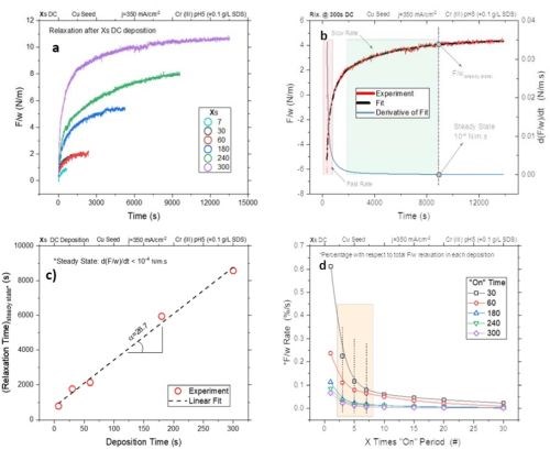
Figure 1 - F/w transients during the relaxation stage for chromium films DC-deposited for different lengths of time: (a) relaxation transient of the films; (b) an example of an F/w transient, the exponential decay fit, and the rate F/w for the film with 300 sec deposition time; (c) the F/w of the films at steady state and (d) the F/w rate transient of the chromium films deposited using different duty cycles (ton/toff).
In this experiment, we considered films which were in a steady stress state once the F/w rates slowed to 10-4 N/m.sec. Once the films reached the defined rate, their stress state did not significantly change over a period of hours.
To obtain the objective estimate of elapsed time needed to reach the steady state, each relaxation transient was fitted to an exponential decay model and then, the first derivative of the fit was used to calculate the moment when the relaxation rate drops below d(F/w)/dt < 10-4 N/m.sec. As an example, Fig. 1(b) displays the stress transient fit and the derivative of the fit for chromium film relaxation after 300 sec of deposition. Stages with fast and slow relaxation rates are indicated in Fig. 1(b) using the criterion d(F/w)/dt < 10-4 N/m.sec.
Figure 1(c) summarizes the time needed to reach F/w transients steady state for films with various deposition times. The plot shows a linear increase as a function of the chromium film deposition time. This graph emphasizes the fact that, for longer deposition times, the absolute amount of trapped hydride in the film is larger, and as a result of this, more time is needed for hydride decomposition. Figure 1(c) also suggests that to reach steady state, a relaxation time 27 times longer than the plating time for a particular chromium thin film sample is required. In other words, hydride decomposition, as the major phenomenon controlling the tensile relaxation, takes much longer than the time necessary for its formation during the deposition stage.
However, a design of pulse functions with such long "off" times (small duty cycle) may have no significance in electrodeposition practice. Therefore, there is a need for more practical duty cycles in which a substantial amount of hydride would be decomposed and having some reasonable value of duty cycle for actual electrodeposition.
Figure 1(d) is a normalized F/w change rate transient of chromium films deposited with various "on" times. The X axis in the graph represents the relaxation time, which is equal to a multiple of the "on" time (toff = X•ton). For example, X = 5 for ton = 30 and 60 sec corresponds to 150 and 300 sec of toff, respectively. The Y axis is the normalized value of F/w, which shows the percentile change with respect to the value of the F/w for a particular film for which the steady state was reached.
This presentation allows different runs to be compared for a particular pulse function (an example is shown in the Figure 1(c)). The graph of Fig. 1(d) indicates that the rate of change of F/w for chromium films deposited with various ton values all show the same behavior and approach the steady state at X > 25 sec. The transition region between the fast and slow F/w change rate regimes is highlighted in the graph. It lies around 5X for all films and is independent of the chromium film thickness. Therefore, X = 3 and X = 7 reside in the fast and slow F/w change rate regime, respectively. Accordingly, pulses with Xs "on" and 3/5/7 Xs "off" (corresponding to % duty cycles of 25/16/12.5) were chosen for further study.
The 30-nm films were deposited using these pulse functions to compare the stress state of such deposits. The small thickness was chosen to minimize the contribution of the grain boundary (GB) zipping phenomenon to the state of the stress in thin films. At low thicknesses, grain boundary zipping is not an effective contributor to the stress state of the film. Key contributors to the film stress state are chromium hydride incorporation during the "on" time and the tensile relaxation from hydride decomposition during the "off" time.** By growing thicker films, grains in the film start to merge and grain boundary zipping can become a dominant factor in the net stress of the films.*** This transition is reflected in Fig. 2, where deposition with a (2 - 6) sec (on-off) pulse function (X-3X or 25% duty cycle) is shown. The first few pulses result in compression (inset of Fig. 2) but over an extended deposition time (thickness), the film develops a tensile stress as a result of grain growth and subsequent grain boundary zipping.
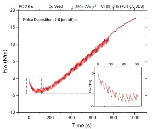
Figure 2 - Stress (F/w) evolution of a film deposited with a duty cycle of 25%: (2 - 6) sec (on-off) pulse. The film exhibits overall tensile stress over time. However, the graph inset shows compressive stress at the early stage of deposition where grain boundary zipping is not effective.
Figure 3 shows the stress state of 30-nm films deposited through various pulse functions with relaxation time being toff = X•ton where X = 3/5/7. At the early stage of deposition with a duty cycle of 25% (X = 3), the growth stress of the films is negative for all pulses (ton). This behavior is rooted in the fact that toff = 3•ton relaxation time lies in the rapid F/w relaxation rate region (Fig. 1). In other words, a significant amount of trapped hydrides has no opportunity to decompose from the film with such a duty cycle and the net stress state of the film remains compressive. Increasing toff in the pulse function where X = 5 (decreasing the duty cycle to 16%), allows for more hydride removal and therefore leads to reduced compression in the films. In this way, some chromium films show tensile stress for ton ≥ 0.5 sec. As expected, films deposited with toff = 7•ton (12.5% duty cycle) have shown the highest value of positive stress. They all show tensile stress except for the films produced with ton =0.1. These results are in agreement with the data in Fig. 1, in which X = 7 is in the region of the F/w relaxation rate where stress values are approaching a steady state.†
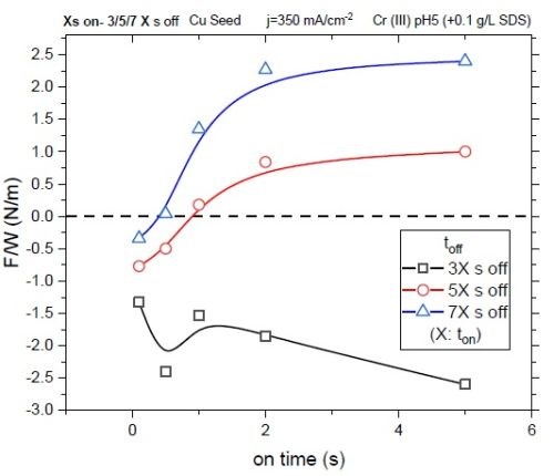
Figure 3 - Stress state of 30-nm films deposited with various pulse functions with duty cycles of 25, 16 and 12.5%.
Potential transients during short current pulses can explain the lower tensile stress in films that are deposited with short ton (ton = 0.1 sec and 0.5 sec). Figure 4 shows the potential transient during deposition (Fig. 4(a)) and relaxation (Fig. 4(b)) of pulses with 50% duty cycle. The data suggest that the effective deposition potential and relaxation potential are reached only for "on" and "off" times longer than 1 sec - in other words, when the chromium films reach a steady state value of the potential. Therefore, the efficient deposition or decomposition of hydride require a suitable electrode potential. This condition for short cycles - particularly less than 1 sec - is not satisfied; for relaxation, the pulses of less than 1 sec do not provide enough time to reach the steady rest potential.
For deposition, the "on" time should be designed in such a way that the majority of the current contributes to Faradaic reaction and not to charging the interfacial double layer. From Fig. 4(a), at least 1 sec is needed to charge the double layer and to reach the steady deposition potential (about -2.2 VAg/AgCl). Therefore, an effective "on" time is one larger than 1 sec.
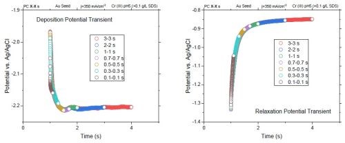
Figure 4 - Potential transients in (a) deposition and (b) relaxation of various pulses with a 50% duty cycle.
Figure 5 shows the EQCM data for the deposition efficiency of chromium films deposited with a duty cycle of 50% and various pulse lengths. This graph indicates that deposition efficiency drops to below 60% for pulses of 0.1 sec in length (ton = 0.1 sec), where a significant portion of the current corresponds to charging of the double layer (non-Faradaic current).
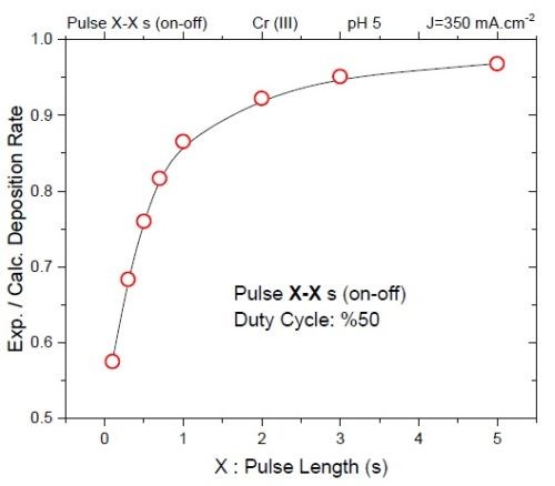
Figure 5 - Deposition efficiency of various pulse lengths with a 50% duty cycle.
Considering Figs. 4 and 5, a lower tensile stress for pulse lengths of ton = 0.1 sec and 0.5 sec can be explained as a consequence of an inefficient deposition / relaxation process. The significance of this data is that it shows that there is a lower limit for designing the deposition and relaxation times. Pulse current lengths and relaxation time (ton and toff) should be designed to satisfy the kinetics of the chromium deposition and hydride decomposition, i.e., a necessary time for the electrode to acquire the steady state potential. The data show an effective strategy for pulse current design which leads to successful hydride decomposition / removal from chromium films. Although the relaxation time, toff, for complete removal of the hydride exceeds 25•ton, the data suggest that chromium films are mostly hydride-free after toff = 7•ton. Both the stress state of film deposited with various ton and potential transients indicate that there is a lower limit for deposition and relaxation time below which the film does not reach the potential for effective chromium deposition and hydride decomposition.
Palladium deposition and stress control
As discussed in the previous report (http://short.pfonline.com/NASF18Nov1), palladium films, during deposition from acidic solutions, develop a huge compressive stress due to the formation of palladium hydride. It has been shown that the use of 0.001M Pb+2 can suppress the hydrogen evolution reaction and significantly mediate the compressive stress in palladium films. The idea behind using solutions containing lead ions is in the formation of an underpotential deposited (UPD) monolayer of lead which floats on top of the growing palladium film and suppresses hydrogen evolution. However, an unreported phenomenon of Pb-Pd codeposition at potentials more positive than the reversible potential of lead has been observed. This phenomenon results in considerable lead content in the deposited palladium films. In this report, a solution with a higher lead ion content was studied to see its effect on the stress state and the composition of the palladium films.
Solution #3: 10-3M Pd+2 + 10-3M H+ + 0.1M Pb+2
Figure 6 shows the F/w transients of the palladium film for multi-step deposition from solution #3 with 0.1M Pb+2 content. As expected, as with Solution #2 with 0.001M Pb+2, which is discussed in the previous report, the addition of 0.1M Pb+2 to the depositing solution significantly reduced the compression at potentials below -0.2 V. However, unlike Solution #2, in Solution #3, the palladium film develops tensile stress at potentials below -0.36 V, where lead overpotential deposition (OPD) is the dominant reaction. This means that the tensile stress is caused by the growth and zipping of Pb-rich grains in the film. Massive lead OPD at potentials below -0.36 V is reflected in Fig. 7(a) which compares the current data of Solution #2 with Solution #3.
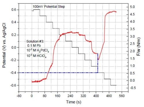
Figure 6 - F/w data of multi-step potentiostatic deposition for Solution #3 containing 0.1M Pb+2.
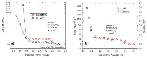
Figure 7 - (a) Comparison between current transients of Solutions #2 and #3; (b) deposition rate of films deposited at various potentials and comparison to the values of the associated current signal. A significant increase in current and deposition rate occurs in the lead OPD case for Solution #3.
The dramatic increase of current below -0.4 V for Solution #3 can be related to the onset of the bulk deposition of lead. However this current increase is not substantial for Solution #2 where the calculated reversible potential of lead and the ratio of Pb:H:Pd were -0.42 V and 1:1:1, respectively.
Employing an electrochemical quartz crystal microbalance (EQCM) to measure the rate of deposition at various potentials (Fig. 7(b)) confirmed that the current change is caused by lead deposition and not hydrogen evolution. This is evident if one considers a huge increase of deposition rate (mass change rate) at potentials below -0.36 V.
More detailed study of the stress-state of the films at various deposition conditions is shown in Fig. 8. Figures 8(a) and (b) show that, starting from positive potentials, the palladium films first develop a tensile stress and then show a slight compressive relaxation at more negative potentials (-0.1 to -0.3 V) at the later stage of the deposition. The trend until -0.3 V is the same as with the other solutions. However, at potentials more negative than -0.4 V, palladium films show a surprising tensile relaxation. We suspect that this behavior originates from concurrent lead OPD, which is the dominant reaction on the surface because of the much higher lead concentration versus that for palladium ions. By going more negative in potential, the film shows compressive relaxation again. Figure 8(c) compares the two sets of experiments. Although the sets have a different deposition times, they demonstrate the same trend. Comparison of stress evolution versus deposition potentials for all three solutions is plotted in Fig. 8(d). Palladium films obtained from Solution #1 with no Pb+2 show a huge compression as the deposition potential enters the hydrogen evolution regime. The presence of 0.001M Pb+2 in Solution #2 significantly decreases the compression and the deposited films just show slight compression at potential below -0.4 V. For Solution #3 with a higher concentration of Pb+2, the palladium films do not experience net compression at any of the applied potentials.
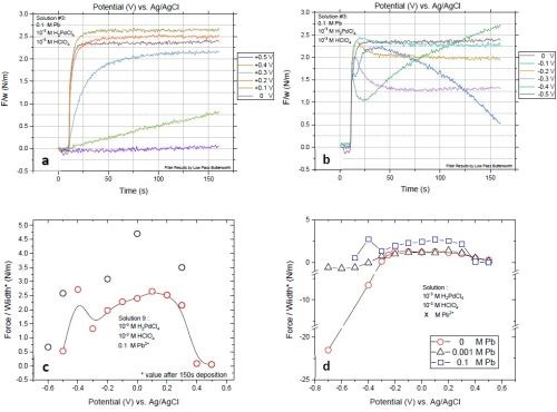
Figure 8 - Stress state of films deposited with various potentials from Solution #3. F/w transients of the films deposited with potentials in the range of (a) +0.5 to 0 V and (b) 0 to -0.5 V; (c) comparison of final values of F/w for two sets of measurements with 150 and 300 sec of deposition time; (d) comparison of the F/w values as a function of deposition potentials for Solutions #1, #2 and #3.
The data in Fig. 8 indicate that the presence of 0.1M Pb+2 significantly changes the stress state of the palladium films. However, as seen in the case of Solution #2, codeposition of lead and palladium in the underpotential region of lead also occurs for Solution #3. The composition of palladium films obtained with solutions containing lead ions is presented in Fig. 9. Solution #2, with 0.001M Pb+2, shows a sudden increase in the lead content of the film at potentials below -0.3 V. This jump in the lead atomic concentration in the films deposited from Solution #3 (0.1M Pb+2) is shifted to a more positive potential. This shift is rooted in the +60-mV shift of the reversible potential for the bulk deposition of lead based on the Nernst equation. Aside from the shift, there is no significant change in the composition of the film at potentials more positive than -0.2 V, which is in the underpotential region of lead. This result suggests that the codeposition of lead at such potentials is potential dependent and is less influenced by the concentration of the Pb+2. More analysis and modeling of the underpotential codeposition process of lead and palladium is necessary to gain a full understanding for composition control in this system.
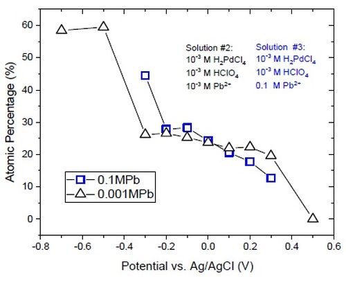
Figure 9 - Comparison of atomic% of lead in the film deposited from Solutions #2 and #3.
Conclusion
In this reporting period, we have shown the effective approach to determine a practical parameters of the pulse current deposition process which leads to chromium thin film deposition with minimum amount of hydride phase, i.e., minimum tensile relaxation. The conclusions are based on combined in situ stress measurements and potential transients. They indicate the effective design of the length for the pulse current stage and the design of the length for the current-off stage. It still remains to be verified if the conclusions based on the stress state of chromium films are compatible with their improved mechanical properties and functionality. These measurements are in planning as collaborative work with Dr. Hall of Faraday Technology.
We have also shown that a lead UPD monolayer growing on the palladium surface can be used as hydrogen evolution suppressor and thus a stress control agent. Yet, the unexpected Pb-Pd underpotential co-deposition phenomenon we have discovered shows the limitation of this approach when the purity of palladium films is considered. An optimum lead ion concentration in the palladium solution that leads to minimum amount of lead incorporation in the palladium films and a palladium films with relatively low level of stress still remain to be found. These data will be reported in the next cycle.
Past project reports
1. Quarter 1 (January-March 2016): Summary: NASF Report in Products Finishing; NASF Surface Technology White Papers, 81 (2), 12 (November 2016); http://short.pfonline.com/NASF16Nov2.
2. Quarter 2 (April-June 2016): Summary: NASF Report in Products Finishing; NASF Surface Technology White Papers, 81 (3), 14 (December 2016); http://short.pfonline.com/NASF16Dec2.
3. Quarter 3 (July-September 2016): Summary: NASF Report in Products Finishing; NASF Surface Technology White Papers, 81 (4), 12 (January 2017); http://short.pfonline.com/NASF17Jan2.
4. Quarter 4 (October-December 2016): Summary: NASF Report in Products Finishing; NASF Surface Technology White Papers, 81 (8), 16 (May 2017); http://short.pfonline.com/NASF17May2.
5. Quarter 5 (January-March 2017): Summary: NASF Report in Products Finishing; NASF Surface Technology White Papers, 81 (11), 12 (August 2017); http://short.pfonline.com/NASF17Aug1.
6. Quarter 6 (April-June 2017): Summary: NASF Report in Products Finishing; NASF Surface Technology White Papers, 82 (4), 10 (January 2018); http://short.pfonline.com/NASF17Jan1.
7. Quarters 7-8 (July-December 2017): Summary: NASF Report in Products Finishing; NASF Surface Technology White Papers, 82 (9), 10 (June 2018); http://short.pfonline.com/NASF18Jun1.
8. Quarters 9-10 (January-June 2018): Summary: NASF Technical Papers in Products Finishing; NASF Surface Technology White Papers, 83 (2), 17 (November 2018); http://short.pfonline.com/NASF18Nov1.
About the author

Dr. Stanko R. Brankovic is a Professor in the Electrical & Computer Engineering and Chemical & Biomolecular Engineering Departments, as well as Associate Director, Center for Integrated Bio and Nanosystems at the University of Houston, Houston, Texas. He holds a B.E. in Chemical and Biochem. Eng. from the University of Belgrade, Serbia (1994) and a Ph.D. in the Science and Eng. of Materials from Arizona State University, Tempe, AZ (1999). He is active in many professional societies, including serving as Vice-Chair and member of the Electrodeposition Division Executive Committee of The Electrochemical Society (2006‐present) and as the Chair of the Electrochemical Material Science Division, The International Society of Electrochemistry (2015‐2017). His research interests include electrodeposition, thin films, electrocatalysis, sensors, corrosion and electrochemical material science and nanofabrication.
*Corresponding author:
Dr. Stanko R. Brankovic
Associate Professor
Department of Electrical & Computer Engineering
Department of Chemical & Biomolecular Engineering
Department of Chemistry
N 308 Engineering Building 1
Houston, Texas 77204-4005
Phone: (713) 743-4409
Fax: (713) 743-4444
E-mail: srbrankovic@uh.edu
** Here the effect of Laplacian pressure on small grains, at early stage of film growth, is neglected.
*** In thick films, competition between the tensile stress from grain boundary zipping and compression from hydride incorporation decide the net stress of the film.
† As an example, in the case of a 300-sec deposition, 85% of the total tensile relaxation occurred by 2100 sec (7X).
RELATED CONTENT
-
Hybrid Sol-Gel Coatings in Surface Engineering
A look at the use of modified sol-gel polymer films and hybrid system coatings, as well as the methodologies for evaluating the mechanical properties of the coatings.
-
Cyanide-Free Electroplating of Cu-Sn Alloys
This paper is a peer-reviewed and edited version of a presentation delivered at NASF SUR/FIN 2012 in Las Vegas, Nev., on June 13, 2012.
-
The Study of Copper Anodes in Acid and Cyanide Plating Baths
The 1956 Carl E. Huessner Gold Medal Award was given to Charles Faust and William H Safranek for Best Paper appearing in Plating or the AES Technical Proceedings in 1955, and their paper is republished here in a series on the AES/AESF/NASF Best Paper Awards. Their work involves an evaluation of anodes for copper plating at the time when OFHC anodes were first emerging in use.


