Crack Formation during Electrodeposition and Post-deposition Aging of Thin Film Coatings - 4th Quarterly Report
Fourth Quarterly Report - AESF Research Project #R-118. This NASF-AESF Foundation research project report covers the fourth quarter of project work (October-December 2016).
#research #nasf
by
Prof. Stanko R. Brankovic*
Featured Content
University of Houston
Houston, Texas, USA
Editor’s Note: This NASF-AESF Foundation research project report covers the fourth quarter of project work (October-December 2016) on this AESF Foundation Research project at the University of Houston. Access information to past project reports referred to in this paper is listed at the end of this report. A printable PDF version of this report is available by clicking HERE.
Personnel:
- Stanko R. Brankovic, PI, Electrical and Computer Engineering and Chemical and Biomolecular Engineering, University of Houston,
- Kamyar Ahmadi, PhD Student, Material Science Program, University of Houston,
- Nikhil Chaudhuri, PhD Student, Material Science Program, University of Houston.
Objective
The objective of the proposed work is to study fundamental and practical aspects of crack formation in electrodeposited thin films. The aim is to identify and quantify the key parameters of the electrodeposition process affecting the crack formation in thin films. This study should enable development of an effective strategy generally applicable in practice whenever electrodeposition process for crack-free films is demanded.
The activities in this period were focused on studies of stress evolution in chromium thin films, ~8 microns in thickness deposited on 1 micron of copper on 100 nm NiCr seed (Cu/NiCr seed), during aging at room temperature in air and during annealing at 250°C in air. The chromium films were deposited from Cr+3-containing electrolytes (EXDBA 1411 Bath at pH 5). In parallel to the in situ stress measurements, complementary impedance measurements of chromium thin films during relaxation in air at room temperature and during annealing at 250°C have been performed for the same temperature range and ramping rate.
Experimental approach
In situ stress measurements
Room temperature relaxation of chromium films deposited from EXDBA 1411 Bath at pH 5, on Cu/NiCr seed
The one issue that had to be addressed from our previous report (3rd Quarterly Report) was the complete comparability among the samples for air and annealing studies. In that report, the air relaxation experiment was performed on the samples that were deposited on copper seed, which is much more conductive than Cu/NiCr (rest of the samples) but with poorer adhesion. Therefore, small changes in the copper seed conduction/delamination during the aging process could be the reason for the large impedance change during air aging that we observed. For this reason, a set of new in situ stress and impedance measurements was performed on chromium films deposited on 1 micron Cu/20 nm NiCr (Cu/NiCr) seed during air aging, representing the same situation as in our annealing studies at 250°C; fast ramping rate, (see previous report). The resulting in situ stress data are shown in Fig. 1(a), for chromium films of ~8 micron thickness. A comparison between the data obtained on chromium films deposited on copper seed (previous report) and chromium films on Cu/NiCr seed (this report) is shown in Fig. 1(b).
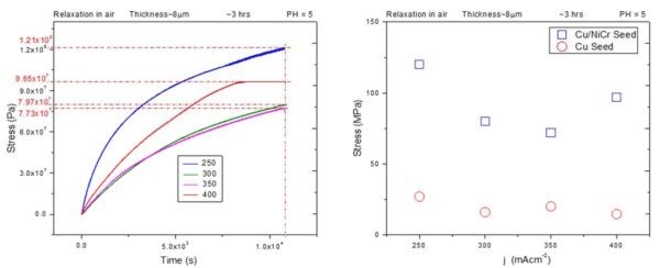
Figure 1 - (a) In situ stress transients during room temperature aging of ~8 micron thick chromium films deposited on Cu/NiCr seed at different current densities used for chromium deposition; (b) comparison between the maximum stress observed during room temperature aging of chromium films deposited on copper seed (red) and Cu/NiCr seed (blue).
Qualitatively, the stress transients have the same shape for chromium films deposited on Cu/NiCr and copper seed (previous report, Fig. 5). They exhibit a continuous rise with time but in the case of the Cu/NiCr seed, no steady stress state is reached. The comparison between the maximum stress values observed after 3 hr of room temperature aging in air for these two sets of samples indicates that tensile relaxation in chromium films in the case of Cu/NiCr seeds reaches much higher values. They range between ~120 MPa for 200 mA/cm2 to ~71 MPa for 350 mA/cm2. The maximum stress versus deposition current dependence exhibits a pronounced minimum for the 350 mA/cm2 sample (Fig. 1(b), blue). This differs from what we have seen in the case of chromium films deposited on copper seed, which had more less a constant value. Therefore, the nature of the seed layer, its adhesion to the glass substrate, as well as the deposition current have a significant effect on room temperature stress relaxation in chromium films deposited form Cr+3-containing electrolytes. Further analysis of this data will be addressed later in the text after presenting the in situ impedance measurements for the chromium films during room temperature aging in air.
Relaxation of chromium films deposited from the EXDBA 1411 Bath at pH 5, on Cu/NiCr seed during 250°C annealing, at a slow temperature ramp rate (1.6°C/min).
The in situ stress and temperature transients recorded during 250°C annealing of ~8 micron thick chromium films deposited on Cu/NiCr seed are shown in Fig. 2(a-d). The temperature profile involved three steps. The first step involved a slow ramp rate of 1.6°C/min for two hours to reach 250°C. Second is a one-hour hold at 250°C. The third step is a subsequent temperature decrease with at a rate of approximately ‐3°C/min to room temperature (Fig. 2). The observed stress transients show a common behavior, in that the stress rises (tensile relaxation) during temperature ramping, then it shows small change or remains constant during the temperature hold, and then remains constant or shows a small compressive relaxation during cooling. The annealing process produces a significant appearance of defects in the films in the form of blistering, cracking and partial delamination.
Optical images of the cantilevers are shown as insets in Fig. 2. It is obvious that the annealing process produced irreversible changes in the stress state of the chromium films. A tensile relaxation of 200-350 MPa was observed. These values are close to the ultimate tensile strength for chromium films (200‐250 MPa). The largest degree of relaxation is observed for chromium films produced at a current density of 350 mA/cm2. A closer inspection of the stress transients shows that there were occasional discontinuities, indicative of thin film cracking (Fig. 2a & d). The qualitative tensile relaxation behavior also indicates that the stress state in the chromium films was mostly influenced by the solid state processes in the film rather than by thermal stress developed from the different thermal expansion coefficients of metal and glass. In each of the measurements, the stress increase is not a monotonic function of time for a constant temperature or temperature ramping rate, but rather a more complex behavior. The observed irreversibility in the stress state on cooling is one more indication that the structure of the chromium films was changed.
One important observation to note is that the noise in the data increases during the holding stage (2nd state, T = constant), which could mean that the fluctuations in the stress‐time data are indeed related to the formation of microcracks. The tensile relaxation produced by the annealing process is larger than that for either room temperature (RT) aging in solution or in air. We will return to analysis of this data later in the text after presenting the impedance results.
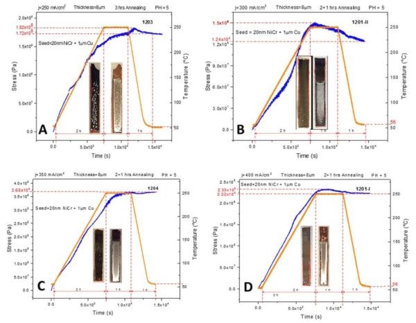
Figure 2 - In situ stress and temperature transients of 8-micron chromium films deposited on Cu/NiCr seed during 250°C annealing: (a) j = 200 mA/cm2, (b) j = 300 mA/cm2, (c) j = 350 mA/cm2 and (d) j = mA/cm2. The optical images show the representative appearance of the chromium films on glass cantilevers after annealing.
Relaxation of chromium films deposited from the EXDBA 1411 bath at pH 5, on Cu/NiCr seed during 250°C annealing, at a rapid temperature ramp rate (50°C/min).
In order to complement the impedance data provided in previous report (3rd Quarterly Report, Fig. 4(a-d)), we performed in situ stress measurements on 8-micron chromium films deposited on Cu/NiCr seed using the identical temperature profile from the previous report. This includes a fast temperature ramp rate of 50°C/min, followed by 2 hr at the 250°C temperature hold, then cooling at a rate of ‐3°C/min. All stress transients showed a complex behavior, as in Fig. 3(a-c).
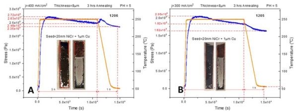
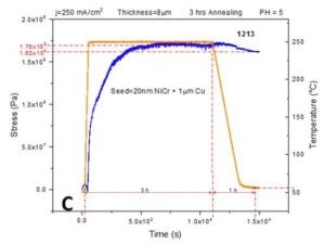
Figure 3 - In situ stress and temperature transients for 8-micron thick chromium films deposited on Cu/NiCr seed during 250°C annealing: (a) j = 400 mA/cm2, (b) j = 300 mA/cm2 and (c) j = 250 mA/cm2. The temperature ramp rate was 50°C/min, while the cooling rate was ‐3°C/min. The time interval for holding at T = 250°C was 2 hr. The overall length of each interval is indicated in each graph.
The rapid temperature ramp rate is matched by a rapid tensile relaxation, reaching values between 170 and 270 MPa. Tensile relaxation does not rise monotonically with time and temperature but rather shows a dependence with the changing slope. In particular, an interesting result is that the change in the slope of the stress‐time data occurs at the moment when the temperature reaches above a range of 150‐175°C. The compressive relaxation is observed as the maximum tensile stress is reached during the temperature hold at 250°C, and during the cooling stage. The sample deposited at 250 mA/cm2 shows somewhat different behavior. The tensile relaxation was more gradual, extending to the region of constant temperature, while the compressive relaxation during that stage was almost negligible. The overall comparison between the maximum levels of tensile stress developed during annealing of the chromium samples using two different temperature profiles (Fig. 2 vs. Fig. 3) indicates similar values for samples deposited at 250 and 400 mA/cm2, while the largest discrepancy was observed for samples deposited at 300 mA/cm2 (Figs. 2b & 3b). The same trend was also observed when comparing the impedance data, as will be discussed next.
Impedance measurements
Resistance/impedance change of chromium films exposed to air during room temperature aging
During this quarter, we performed in situ impedance measurements during chromium film aging in air at room temperature and during annealing at 250°C. The impedance measurements for aging in air represent a repetition of the measurements from the last report while here the chromium films were grown on Cu/NiCr seed, allowing direct comparison with other measurements and complementing our stress data. The experimental apparatus for in situ room temperature impedance measurements and sample configuration have been described in detail in previous reports (2nd and 3rd Quarterly Reports). The observed resistance changes during room temperature aging for chromium films deposited at different current densities are shown in Fig. 4(a-d). The optical images of the representative morphology of the chromium surface for each transient sample are also shown as insets. Impedance transients were recorded over time intervals of 3 hr, while the approximate chromium film thickness was around 8 microns. The maximum change in the impedance value is indicated in the graph. It ranges from 5% to 25%.
The impedance change with respect to the deposition current density shows a bell-like shape dependence (Fig. 4 and the summary plot of Fig. 6(a)). The maximum change is observed for deposition current densities of 300 and 350 mA/cm2. The common feature of all results in Fig. 4 is the presence of quite pronounced discontinuities manifested as: random impedance jumps, and sudden abrupt increases or decreases as the aging process progresses. Optical inspection of the chromium samples does indicate that no crack formation occurred in the chromium films. However, a sudden change of impedance is characteristic for each of the transients and is indicative of significant structural change within the chromium films. Perhaps, these impedance changes could have arisen from the formation of microcracks not detectible by optical microscopy, or via some phase transformation that could be related to the disintegration of Cr‐hydride upon deposition and its conversion to Cr‐oxide and H2O when in contact with oxygen from air.
One important observation is that in each transient, immediately upon completion of the deposition process and after the solution is drained to start impedance measurements, a common decrease is observed (Fig. 4(a-d)). Depending on the sample, the time varies until the subsequent onset of impedance increase is observed. Yet, this is an indication that the initial dominant process occurring in the chromium films on deposition is qualitatively different than the ones dominating/occurring later due to exposure to air. One explanation could be that the Cr-hydride in the chromium film is stable only when the significant overpotential for H2 evolution and H-radical exist near the surface. In our case, for each sample this occurs during deposition since the potential transients are well below the water electroreduction potential (see 1st report). When the electrodeposition is stopped, the Cr‐hydride starts to decompose, leaving products of chromium and H2 in the film. The latter is trapped within the grain boundaries or within the grains as dissolved interstitials. Hydride disintegration results in decreased resistivity of the chromium films since metallic chromium is likely a better conductor than Cr‐hydride. Later on, in contact with O2, hydrogen as well as chromium react, forming Cr‐oxide which is the process that produces higher resistivity. Since no cracks are observed in the optical microscopy, it is unclear if these two stages result in cracking of the films during room temperature aging. The stress data shown in Fig. 1 do not indicate an abrupt change in stress but rather a gradual tensile relaxation, which can be explained by Cr‐hydride decomposition. Yet, void formation and microcrack generation cannot be excluded.
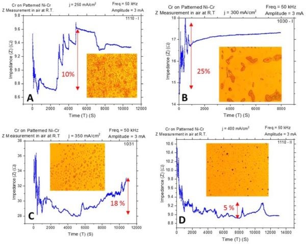
Figure 4 - In situ impedance measurements of 8-micron chromium films during aging at room temperature in air. The impedance of the chromium films was monitored for ~3 hr and the maximum percentage change of impedance from absolute minimum to the maximum over time is indicated. Samples were deposited at (a) j = 250 mA/cm2, (b) j = 300 mA/cm2, (c) j = 350 mA/cm2 and (d) j = 400 mA/cm2. Optical images were taken from the center of the sample; AC amplitude 3 mV, frequency 50 kHz.
Resistance change of chromium films exposed to air during annealing at 250°C using a slow temperature ramp rate of 1.6°C/min.
The in situ stress measurements made during chromium thin film annealing at 250°C using a slow temperature ramp rate (Fig. 2) were complemented with the impedance measurements as well. The temperature profile, ramp rate (1.6°C/min) and film thickness were the same. The results are shown in Fig. 5(a-d). The common feature observed on all impedance transients is that the temperature increase (2 hr) is associated with initial decrease of impedance/resistance of the chromium films, while the further temperature hold (1 hr), and cooling step (‐3°C/min), are associated with increase of the chromium film impedance. The described regions are identified in the graphs by the presence of bordering red lines.
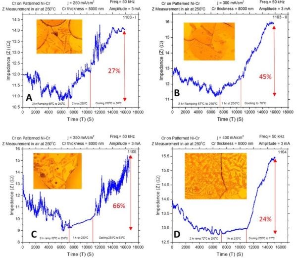
Figure 5 - In situ impedance measurements of 8-micron chromium films during annealing at 250°C in air. The impedance of the chromium films was monitored for ~3 hr and the maximum percentage change of impedance from absolute minimum to the maximum from the increasing trend is indicated. Samples were deposited at (a) j = 250 mA/cm2, (b) j = 300 mA/cm2, (c) j = 350 mA/cm2 and (d) j = 400 mA/cm2. Optical images were taken from the center of the sample; AC amplitude 3 mV, frequency 50 kHz.
The optical images of the chromium film surfaces indicate the appearance of the cracks. Therefore, the common feature of the impedance transients, such as sudden discontinuities and increasing/decreasing spikes, could be attributed to microcracking and some additional structural changes in the chromium films.
The maximum percentage impedance change measured from the absolute minimum to the apparent maximum obtained due to a rising part of the transient are indicated in the graphs. The summary of this data is presented in Figure 6(a). If one compares these transients (Fig. 5) with the stress transients (Fig. 2), it seems that tensile stress relaxation is associated with the overall decrease in impedance of the chromium films. The further small compressive relaxation during the temperature hold or cooling steps is associated with the overall increasing impedance of the chromium films.
We have already discussed that the possible mechanism for defect formation during room temperature aging of chromium film involved the decomposition of CrxHy (Cr‐hydride) in the bulk phase. This process can liberate the hydrogen molecules (CrxHy = 0.5yH2 + xCr) which are trapped within the bulk of the sample at the grain boundaries, or in the lattice, allowing gas molecules to agglomerate and create a nano‐voids. They represent structural imperfections, and thus can act as electron scattering points. Hydride decomposition should also be associated with tensile stress relaxation in the films1 during aging in air at room temperature. We do observe this phenomenon, which is also associated with the initial impedance decrease resulting from hydride decomposition (Figs. 1 and 4). However, during annealing, the tensile stress relaxation in the film could result in the formation of additional transport pathways for oxygen molecules to reach trapped hydrogen and form water, and to reach chromium liberated from the Cr‐hydride to form Cr‐oxide. Therefore we can expect H2O formation and chromium oxidation as the main chemical change during annealing. They cannot be excluded during the room temperature aging in air as well, but it is likely that hydride decomposition is the dominant process. In terms of the stress signature of annealing, increasing the temperature should help to liberate H2O from the chromium deposit for temperatures >100°C, and thus a decreased film resistance is expected by removal of electron scattering phase.
We can therefore hypothesize that the tensile stress associated with the temperature rise during annealing is governed by hydride decomposition and water losses. Both are responsible for the decrease in the resistance of the chromium film (Fig. 5). At higher temperatures, chromium liberated from hydride and potentially the chromium in the metallic state that is deposited are subjected to oxidation by oxygen from air penetrating through the porous grain boundaries where hydride and water have been removed. The oxide formation as a phase with a larger volume than that of the original metallic chromium contributes to compressive relaxation (Fig. 2). This is what we observed in our experiments. Oxide growth in the chromium films is the likely reason for the observed increase in impedance during temperature hold and cooling steps (Fig. 5).
Summary
In our first year of working on the problems of thin film cracking in chromium deposits obtained from trivalent solutions, we have developed a good understanding of the fundamental origins of this process. First, we have developed a methodology for in situ stress measurements and in situ impedance measurements of chromium films, which allows us to monitor indirectly the crack formation in chromium films during deposition, aging and annealing. This was of crucial importance to distinguish different processes in the chromium films that contribute to their stress state, mechanical integrity, cracking and change in their electrical properties. Our work presented in first six months (1st and 2nd Quarterly Reports) clearly demonstrated that cracking in chromium films is not likely to occur during electrodeposition.
The observed growth stress was negative, i.e., compressive with steady state values in the range below ‐100 MPa. Yet, we observed blistering in the chromium films and an accumulation of different defects on the chromium film surface during deposition which indicated a significant amount of dissolved hydrogen either as an interstitial impurity or as a part of chemically-bonded hydrogen as a Cr‐hydride.
The formation of metal‐hydrides is exclusively associated with the compressive stress in metal films, and this conclusion is adopted in our case. Our electrochemical measurements were in concert with this conclusion, as we have determined that, during deposition, the rest potential of the chromium films is well below the electrochemical water splitting potential where the H‐ion species are present at the metal‐solution interface. Thus, one could expect a significant amount of metal‐hydride formation and hydrogen dissolution in the chromium films, as noted in the first two quarterly reports.
Further studies have focused on the stress state in the chromium films during aging process in solution, in air and during annealing at 250°C. The summary of these data is shown in Fig. 6. Our studies clearly indicate that the tensile relaxation in the chromium films is directly related to the environment to which the chromium films are exposed. During relaxation in the solution, which could be considered as an oxygen deprived environment, the maximum change of stress observed was very modest, over the course of several hours (Fig. 6(b)). This modest tensile relaxation was most likely associated with decomposition of the Cr‐hydride phase once the potential for hydrogen evolution and the presence of hydrogen ions was removed. However, we expect that the hydrogen gas molecules released from the hydride phase remains trapped in the deposit as an atomic interstitial, or as gas phase in microvoids formed at the grain boundaries, or within the grains which can act as the crack nucleation sites.
Yet, a small level tensile stress seems insufficient to induce stable crack growth during room temperature relaxation in the electrolyte. The stress level results are also complemented by our impedance measurements of the chromium films during relaxation in solution, which show very modest change in resistance. The disappearance of the hydride phase does not seem to be the main driver of the change in electrical properties (Fig. 6(a)). However, chromium films aged in air/oxygen showed much greater tensile relaxation and an increase in resistance (Fig. 6(a)). The in situ stress measurements showed no direct indication of crack formation during this process. Yet, the stress levels observed approached the values of fracture toughness for pure chromium films.2
Therefore, the presence of oxygen is found to be fundamentally important for the qualitatively different stress and resistance changes observed in the chromium films during the aging process. We are still evaluating chromium structure and oxygen content and we cannot clearly present the true picture describing the relevant phenomena occurring in chromium films during aging in air. Yet, we are very sure that we have two processes occurring in parallel, each contributing to the particular stress and fracture behavior of chromium films: (1) hydrogen oxidation and (2) chromium oxidation. Trapped hydrogen in the chromium films is converted into H2O, which is either trapped in the structure of the chromium films, or at the grain boundaries where it readily escapes to the atmosphere. The latter case also promotes formation of grain boundary pores and defects which contribute to very low fracture toughness in the chromium films. The chromium oxidation liberated from the hydride is a process that generates a much larger tensile relaxation, >100 MPa (Fig. 6(b)) and thus represents additional weakening of the grain boundaries if the hydride is formed there, or contributes to additional amorphization of the chromium films if it is formed within the grains. The latter conclusion is also supported by our recent XRD data (not shown in this report) which suggest that chromium films are almost 100% amorphous.
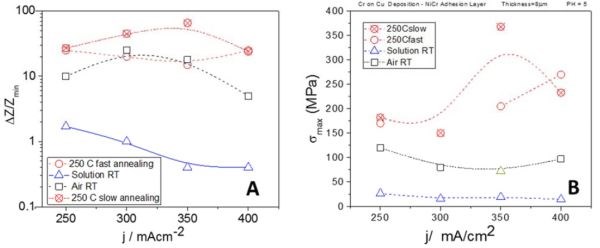
Figure 6 - Summary of (a) in situ impedance measurements, change presented in % units and (b) in situ stress measurements as a function of deposition current density.
Our in situ stress, impedance and optical results undoubtedly suggest that the annealing process is solely responsible for visible crack formation in the chromium films. This is a consequence of the weakened structure of the chromium films by oxidation, which has its true origin in Cr‐hydride formation and the subsequent oxidation of its degradation by‐products (hydrogen and chromium). Although the in situ stress data do not show any catastrophic failure of the chromium films, or brittle fracture propagation that would be an obvious signature of cracking, a closer inspection of the stress data shows that their complex behavior indeed represents an interplay of internal structural changes related to chemical processes, as well as formation of micro- and macrocracks. The observed levels of tensile stress (Fig. 6(b)) in some of our samples are close to or exceed the fracture toughness or ultimate tensile strength of the chromium films (>250 MPa)2 at the temperatures of 250°C. The stress data are in agreement with impedance studies during annealing which also show the largest resistance change. Both measurements qualitatively show the same trend if samples deposited at different current densities are compared (Figs. 6(a) and (b)). Yet, more results and work is necessary to design a fruitful strategy to tackle the problem of cracking in chromium films. One thing for certain is that an electrodeposition process that produces less Cr‐hydride in the deposit should be more desirable when crack-free chromium films is the goal. More progress along this direction is expected in this next year.
References
- S.R. Brankovic, et al., Electrochimica Acta, 83, 387-393 (2012).
- U. Holzwarth and H. Stamm, Journal of Nuclear Materials, 300, 161-177 (2002).
Past project reports
- Quarter 1 (January-March 2016): Summary: NASF Report in Products Finishing; NASF Surface Technology White Papers, 81 (2), (November 2016); http://short.pfonline.com/NASF16Nov2.
- Quarter 2 (April-June 2016): Summary: NASF Report in Products Finishing; NASF Surface Technology White Papers, 81 (3), (December 2016); http://short.pfonline.com/NASF16Dec2.
- Quarter 3 (July-September 2016): Summary: NASF Report in Products Finishing; NASF Surface Technology White Papers, 81 (4), (January 2017); http://short.pfonline.com/NASF17Jan2.
Corresponding author:
Dr. Stanko R. Brankovic
Associate Professor
Department of Electrical & Computer Engineering
Department of Chemical & Biomolecular Engineering
Department of Chemistry
N 308 Engineering Building 1
Houston, Texas 77204-4005
Phone: (713) 743-4409
Fax: (713) 743-4444
E-mail: srbrankovic@uh.edu
About the author:

RELATED CONTENT
-
Electroplated Tin-Nickel Coatings as a Replacement for Nickel to Eliminate Nickel Dermatitis
This paper is a peer-reviewed and edited version of a paper delivered at NASF SUR/FIN 2013 in Rosemont, Ill., on June 12, 2013.
-
Chromium-free Etching and Palladium-free Plating of Plastics
Plastics are replacing metals in the manufacture of many parts, and quite often there is a need for metallic coatings on the plastics and other non-conductors. This paper will describe new processes of preparing ABS plastic substrates for subsequent metallization.
-
Qualitative Approach to Pulse Plating
In 1986, the AESF published Theory and Practice of Pulse Plating, edited by Jean Claude Puippe and Frank Leaman, the world’s first textbook on pulse plating. A compendium of chapters written by experts in this then-emerging field, the book quickly became the authoritative text in pulse plating. What follows here is the opening chapter, serving as an introduction to the field. Although the field has grown immensely in the intervening 35 years, the reader will find that the material remains a valuable introduction to those looking to advance the field of pulse plating.


