Crack Formation during Electrodeposition and Post-deposition Aging of Thin Film Coatings - 5th Quarterly Report
This NASF-AESF Foundation research project report covers the fifth quarter of project work (January-March) on this AESF Foundation Research project at the University of Houston. The objective of the work is to study fundamental and practical aspects of crack formation in electrodeposited thin films.
#nasf #basics
by
Prof. Stanko R. Brankovic*
Featured Content
University of Houston
Houston, Texas, USA
Editor’s Note: This NASF-AESF Foundation research project report covers the fifth quarter of project work (January-March) on this AESF Foundation Research project at the University of Houston. Access information to past project reports referred to in this paper is listed at the end of this report. A printable PDF version of this report is available by clicking HERE.
Personnel:
- Stanko R. Brankovic, PI, Electrical and Computer Engineering and Chemical and Biomolecular Engineering, University of Houston,
- Kamyar Ahmadi, PhD Student, Material Science Program, University of Houston,
- Wenli Yang, PhD Student, Material Science Program, University of Houston.
Objective
The objective of the proposed work is to study fundamental and practical aspects of crack formation in electrodeposited thin films. The aim is to identify and quantify the key parameters of the electrodeposition process affecting the crack formation in thin films. This study should enable development of an effective strategy generally applicable in practice whenever electrodeposition process for crack-free films is demanded.
The activities in this period were focused on structural and compositional studies of chromium thin films, ~ 8 micron in thickness. The chromium films were deposited from Cr+3-containing electrolytes (EXDBA 1411 Bath with pH=5). In addition to these efforts, the work on developing an effective pulse deposition strategy to produce chromium films with minimum amount of hydride phase has started.
Experimental approach
XRD Measurements for chromium films electrodeposited on 100 nm copper and ruthenium seed.
The compressive stress developed in chromium films during electrodeposition process from Cr(III) solutions indicates qualitatively different stress evolution as compared to traditionally seen ones in chromium films produced from Cr(VI) electrolytes (see previous reports). Our in situ stress and impedance studies during annealing of chromium films and during their aging in air (see previous reports) show that the fracturing occurs during postdeposition treatment. The tensile stresses developed during post-deposition treatment are relatively low (<100 MPa), which also indicated that chromium films produced from Cr(III) solutions are characterized with low fracture toughness. These results prompted study of the structure of chromium films using XRD method. The seeds on which chromium films were deposited were copper and ruthenium, 100 nm thick films. These two seeds were chosen to allow complementary investigation of chromium structure avoiding the interference from the peaks related to the substrates. The data are shown in Fig. 1 (copper seed) and Fig. 2 (ruthenium seed). The XRD pattern of the seed layer and chromium film are over layered for each sample so that misreading of the peaks related to the underlying seed is avoided. The chromium films were electrodeposited using current densities in the range from 200 to 400 mA/cm2. The common and somewhat surprising result from these studies (Figs. 1 and 2) is that the metallic part/phase of the chromium films shows no crystallinity. A possible presence of a chromium (110) peak is shown in Fig. 2.
However, a more careful analysis of this peak and comparison to the ruthenium substrate pattern yields inconclusive evidence about any crystallinity of chromium metal phase. Therefore, the XRD results demonstrate that metallic phase of the films does not show any peak pattern in the 2θ scan. The lack of characteristic peaks for the chromium lattice indicates that the coherence length in the metallic phase of chromium films is smaller than ~3 nm. Another surprising result is that the XRD patterns on the chromium films on the copper seed show presence of crystalline Cr-oxide (Fig. 1). The Cr2O3 (012), (104) and (110) peaks are indicated in Fig. 1. The oxide presence in the chromium films could be related to two different processes which have been discussed in our previous reports. The first one is the precipitation of Cr(OH)3 in the chromium film during the electrodeposition process. This type of oxide is expected to have an amorphous structure as seen in oxides in FeCo alloys originating from Fe(OH)3 precipitation. However, the crystalline nature of Cr-oxide in this case indicates most likely that the source of this oxide is different. It is likely that crystalline Cr-oxide is produced upon oxidation of native chromium liberated after Cr-hydride decomposition. Therefore, one expects that structure of metallic chromium and Cr-oxide to be intermixed yielding an overall amorphous appearance of the metallic chromium films where significant portion of the chromium thin film body is comprised of the Cr-oxide.
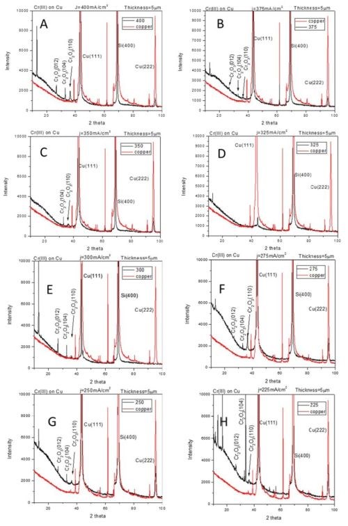
Figure 1 - XRD-2θ scans for chromium films electrodeposited on copper seed using a current density of (A) 400 mA/cm2, (B) 375 mA/cm2, (C) 350 mA/cm2, (D) 325 mA/cm2, (E) 300 mA/cm2, (F) 275 mA/cm2, (G) 250 mA/cm2 and (H) 225 mA/cm2.
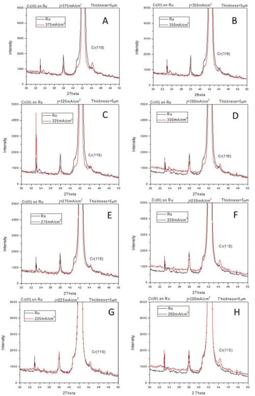
Figure 2 - XRD-2θ scans for chromium films electrodeposited on ruthenium seed using current density of (A) 400 mA/cm2, (B) 375 mA/cm2, (C) 350 mA/cm2, (D) 325 mA/cm2, (E) 300 mA/cm2, (F) 275 mA/cm2, (G) 250 mA/cm2 and (H) 225 mA/cm2.
EDX measurements
The compositional study of electrodeposited chromium films was carried out using Energy Dispersive X-ray Spectroscopy (EDX). The data are shown in Fig. 3 as atomic content of chromium, oxygen and carbon as a function of current density used in electrodeposition process. The common trend that was observed is that higher current density produced chromium films with more chromium and less carbon. Overall a relatively high content of both carbon and oxygen is observed (>15%). The latter is found to have minimal dependence on the current density used in deposition process. However, the carbon content seems to decrease with increasing current density, particularly in the range of 225-300 mA/cm2. This trend seems to mirror the increasing chromium content in the deposit. The plausible explanation for this observation is that carbon in the deposit originates form HCOOH which serves as the ligand for the Cr+3 ion. The rate of HCOOH decomposition and carbon trapping is probably not dependent on the current density as much as on the potential of the electrode surface, which changes very little with increasing current density (see first report). However, the increasing current density leads to a higher chromium deposition rate, and these two combined effects lead to the observed trend in chromium and carbon content. The oxygen in the deposit, as discussed previously, could be originating from two different sources, and thus it could be dependent not only on the deposition rate, but also on the age of the samples (second mechanism via Cr-hydride decomposition and Cr-re-oxidation). The observation that there is no obvious trend on current density could also be a result of the age of the test samples (1 week) where the predominant part of the oxide was formed by native chromium oxidation. Therefore, more studies about the true origin of oxygen are needed to discern the reason for the constant oxygen content in deposit as a function of current density used in the deposition process. The composition of the chromium films will be revisited in the future using nano-EDX mapping of the TEM images where precise spatial distribution of the carbon, oxygen and chromium will be investigated and thus more information about the chromium film structure will be available.
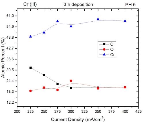
Figure 3 - EDX data for the composition of chromium films as a function of current density. The accuracy of EDX for light elements is ±3%.
Pulse deposition concept and process design
As discussed in the last report, the electrodeposition process that produces less Cr-hydride in the deposit should be more desirable when the crack-free chromium films are the goal. With this in mind, we proceeded with a design of the pulse deposition process where the main goal was to minimize the amount Cr-hydride formation in the deposit. The general idea of this approach is described in the Fig. 4. The current pulse stage (ON stage) of the deposition process is expected to yield the chromium films with similar structure and composition as the ones obtained during DC plating. We chose the pulse current density to be 350 mA/cm2 which produced DC chromium films with best electrical properties. Therefore, in this stage we would expect to see the formation of chromium films with Cr-hydroxide and Cr-hydride phases incorporated in the film matrix as well. However, the OFF stage was designed to allow decomposition of the Cr-hydride over the thickness of chromium film formed in the ON stage. The logic behind this is that we would expect to see decomposition of Cr-hydride once the driving force for H- species formation is removed from the system (once the potential falls below the water reduction potential, E = -1.125 V). The length of the OFF stage was calculated based on the “rough” calculations of hydrogen atomic interstitials in the BCC metal lattice, where the thickness/diffusion path in the layer is assumed to be the one deposited in the ON stage. The basic outline of this pulse current design is shown in Fig. 4, while the parameters of the ON and OFF stage are indicated in each of the figures to follow (Figs. 5 and 6).
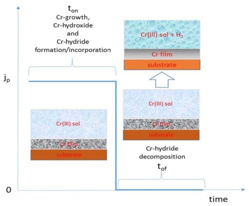
Figure 4 - Schematics of pulse deposition concept and intended results.
Stress relaxation during chromium film aging in solution - pulse current deposition
In this study, we investigated the effect of OFF time on the stress relaxation in chromium films during aging in solution. The ON time was set to be 80 msec for all samples with a pulse current density of 350 mA/cm2. The OFF time was varied between 0 and 20 msec. The growth stress for all samples was found to be compressive and below -100 MPa. The data obtained for stress relaxation on deposition during aging in solution are shown in Fig. 5. It is evident that there is no dependence of the magnitude of stress relaxation on the OFF time. The magnitude of tensile relaxation of all samples is in the range of 60-75 MPa, and most likely the origin of that relaxation is just the volume change (shrinking) of the chromium films due to the breakup of Cr-hydride as a phase which has larger volume than the chromium matrix. To some extent, this is expected, since the presence of oxygen in the solution is very small, ~10-4M. Therefore, Cr-hydride decomposition is likely to yield native chromium which is not quickly re-oxidized. Because of that, the fracture toughness of these films is expected to be higher than for the films exposed to air or films that have undergone annealing. The grain boundaries or defects where the crack nucleation and propagation was expected to happen seem ineffective since the samples showed no sign of fracture. Therefore, we conclude that the OFF time effects were not observed due to a lack of an oxidizing environment, which we introduced in our next experiment.
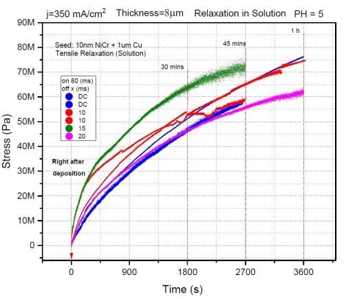
Figure 5 - The effect of OFF time on stress evolution of pulse deposited chromium films during aging in solution; ON time: 80 msec, pulse current density: 350 mA/cm2.
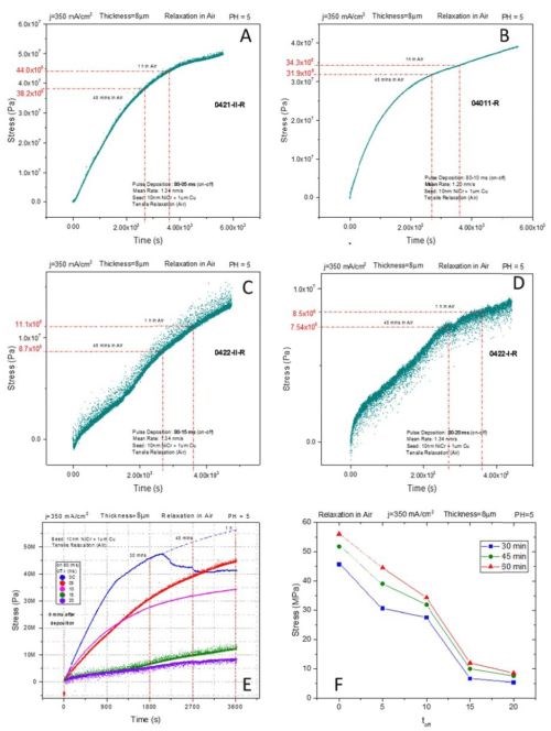
Figure 6 - The effect of OFF time on stress evolution of pulse deposited chromium films during aging in air at room temperature; ON time: 80 msec, pulse current density: 350 mA/cm2. The data in (E) and (F) are the summary of results presented in (A)-(D). For data in (F), sets are formed by observing stress relaxation at three different moments, 30, 45 and 60 min upon deposition of the chromium film.
Stress relaxation during chromium film aging in air - pulse current deposition.
The same experimental logic explained in the previous paragraph was followed during the stress relaxation measurements for samples aging in air. The time of the experiment was one hour. The set of in situ results is shown in Figs. 6A-D, and the data summary is presented in Figs. 6E-F. The OFF time was varied between 5 and 20 msec while the pulse current was 350 mA/cm2 with an ON time of 80 msec. The observed magnitude of tensile stress relaxation was very dependent on the OFF time. As seen in Fig. 6A, the DC sample shows small difference between aging in air and solution, ~55 vs. 70 MPa.
In previous reports we have discussed the effect of an oxygen environment on the tensile stress relaxation/reduction. The metallic chromium formed after the breakup of the Cr-hydride becomes oxidized, and thus the formation of Cr-oxide at the grain boundaries and through the chromium matrix (compressive stress) contributes to lowering of the tensile stress induced by hydride decomposition. However, as the OFF time increases, the magnitude of the tensile relaxation becomes smaller. It gradually decreases from 50 MPa for 5 msec OFF time to <10 MPa for 20 msec OFF time. The observed trend is plotted in Figs. 6E-F for three different aging times for which the stress state was compared among the pulse deposited samples. The idea of introducing OFF time to allow the Cr-hydride break up in between the subsequent growth stages seems to be proven effective.
Yet to be discussed and designed is the best and most optimum approach for choosing the ON time and OFF time. More about this approach will be soon available when our in situ impedance measurements are available for these samples and compared with stress measurements in detail. However, we can say that the data in Fig. 6 are encouraging. They indirectly suggest that introduction of the OFF time leads to reduced Cr-hydride formation and thus its consequent reduced decomposition/re-oxidation during the aging in air. This means that the goal of forming a chromium deposit with less tensile relaxation and better fracture toughness is achieved.
It still remains to perform stress relaxation experiments and in situ impedance experiments during annealing at 200°C to examine if the observed trend will hold. For the moment, it seems that the idea of pursuing pulse deposition of chromium films as an approach to achieve crack-free chromium coatings is on strong ground.
Conclusion
In this period we have revealed important information about the structure of the chromium films. The apparent lack of crystallinity together with a large amount of oxide phase indicates that their fracture behavior resembles more a ceramic type of coating rather than a metallic one. The issues with oxide content and oxide incorporation in the chromium films have to be addressed separately from the ones related to the Cr-hydride decomposition/oxidation. At this stage we do not have a clear strategy for preventing Cr-hydroxide incorporation other than working at higher bath of the bath and perhaps working on a better ligand design. For the case of Cr-hydride formation/decomposition, the preliminary data suggest that a pulse deposition approach is promising. Yet, the optimum pulse current function and the process for a give bath design has yet to be developed.
References
1. S.R. Brankovic, et al., Journal of the Electrochemical Society, 158 (11) D641-D646 (2011).
2. S. Elhalawaty, et al., Journal of Applied Physics, 111, 07A330-07A330-3 (2012).
3. J. George, et al., Electrochimica Acta, 110, 411-417 (2013).
Past project reports
1. Quarter 1 (January-March 2016): Summary: NASF Report in Products Finishing; NASF Surface Technology White Papers, 81 (2), 12 (November 2016); http://short.pfonline.com/NASF16Nov2.
2. Quarter 2 (April-June 2016): Summary: NASF Report in Products Finishing; NASF Surface Technology White Papers, 81 (3), 14 (December 2016); http://short.pfonline.com/NASF16Dec2.
3. Quarter 3 (July-September 2016): Summary: NASF Report in Products Finishing; NASF Surface Technology White Papers, 81 (4), 12 (January 2017); http://short.pfonline.com/NASF17Jan2.
4. Quarter 4 (October-December 2016): Summary: NASF Report in Products Finishing; NASF Surface Technology White Papers, 81 (8), 16 (May 2017); http://short.pfonline.com/NASF17May2.
About the author

*Corresponding author:
Dr. Stanko R. Brankovic
Associate Professor
Department of Electrical & Computer Engineering
Department of Chemical & Biomolecular Engineering
Department of Chemistry
N 308 Engineering Building 1
Houston, Texas 77204-4005
Phone: (713) 743-4409
Fax: (713) 743-4444
E-mail: srbrankovic@uh.edu
RELATED CONTENT
-
Coating Systems with the Best Long-Term Performance
The best protection against corrosion and UV exposure, says Axalta’s Mike Withers, is electrocoat and a super durable powder coating.
-
What is Electrocoating?
E-coat can produce uniform finishes with excellent coverage and outstanding corrosion resistance.
-
Fixing Corrosion Between Anodized Aluminum and Steel
Anne Deacon Juhl, Ph.D., with AluConsult, says Galvanic corrosion is due to an electrical contact with a more noble metal or a nonmetallic conductor in a conductive environment.


