New Uses For Anodized Aluminum Oxide
Anodized aluminum oxide (AAO) has attracted significant interest among the nano-science and engineering research community in recent years. AAO consists of highly aligned nanopores “self-assembled” in a hexagonally close-packed pattern.
By H. Hau Wang Argonne National Laboratory
Presented at the 19th Annual International Anodizing Conference & Exposition, October 5-7, 2010, Montreal, Quebec, Canada. For more information, please visit Anodizing.org
Featured Content
Anodized aluminum oxide (AAO) has attracted significant interest among the nano-science and engineering research community in recent years. AAO consists of highly aligned nanopores “self-assembled” in a hexagonally close-packed pattern. The naturally occurred pore diameter and pore-to-pore distance from anodization range between ~30 to 300 nm and 50 to sub-micron, respectively. These nanopores can be prepared in a simple wet chemistry lab without complicate equipments. The nanopore formation based on the driving force from self-assembly demonstrates beautifully the simplicity and power of the bottom-up approach. The nanopore diameter and pore distance can be well controlled through anodization parameters as well as postanodization chemical etching. These nanopores are highly ordered within a domain with domain size on the order of twenty times the pore-to-pore distance. The AAO films do not exhibit intrinsic long range order.
The chemical composition of the AAO film is primary amorphous alumina (Al2O3). The chemical inertness and the mechanical hardness make the AAO thin films ideally suited for surface protection as well as metal finishing and decorative purposes.
The free standing membranes with different pore sizes are also commonly used for filtration and separation in chemical and biotech labs. The chemical inertness also makes the AAO an ideal template for nanoscale synthesis. Many new and potential applications have emerged in the past few years. Most of these applications do not require long range order in the pore arrays. However, long range order can be established with use of more sophisticated and expensive in both time and expense top-down approach such as photo- and e-beam lithography as well as focused ion beam (FIB). With long range order in the nanopore arrays, more advanced development in electronic and magnetic devices as well as photonic applications are expected in the future. The synthesis, formation mechanism, and new development in AAO will be briefly reviewed here followed by nanofabrication, energy, as well as safety and security applications.
AAO formation and mechanism
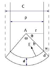
The formation mechanism of AAO membranes was first proposed in the early fifties.1 Key elements of AAO membranes consist of straight nanopores with a spherical bottom less than a hemisphere. The contour of the cell base pattern can be described with a center of curvature and a radius of curvature. The earlier model was expanded significantly in the seventies.2 The revised model is shown in Figure 1. The center of curvature (A) is continuously moving downward during anodization. The active layer during nanopore growth is the bottom barrier layer with thickness (d). There are two active interfaces on the barrier layer. The outer one is associated with anodization of aluminum to alumina, and the inner one associated with Figure dissolution and deposition of alumina to and from the etching solution. The process is driven by the local electric field (E) which is defined by the applied current (I) over conductivity (s) times the surface area of the spherical bottom.
Under a constant applied current (or potential E) and during equilibrium growth, each nanopore reaches an optimized solid angle . and radius of curvature b.3 Each nanopore slowly moves its position with respect to its closest neighbors in order to even out the mechanical stress among them. This self assembly process leads to nanopores with uniform pore diameter and arranged in a two-dimensional hexagonally close packed array. This self-assembly process in AAO formation is a slow process and takes hours to reach equilibrium. A commonly accepted procedure to prepare well ordered AAO membranes is called two-step anodization.4 The concept of the two-step anodization is to first generate aligned nanopores, followed by removal of the initial surface alumina layer.
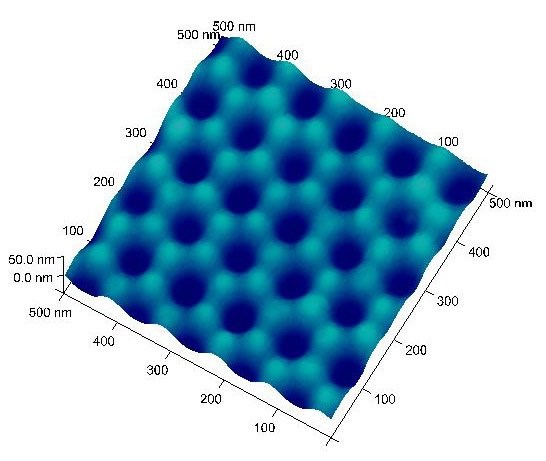
This process generates highly ordered indents on the unreacted aluminum surface. These surface indents serve as the nucleation sites and lead to deep nanopores during the second anodization. Typical Al surface with ordered indents is shown in Figure 2 with indent (pore) diameter around 50 nm and pore-to-pore distance ~110 nm (prepared from 40 V and 0.3 M oxalic acid).
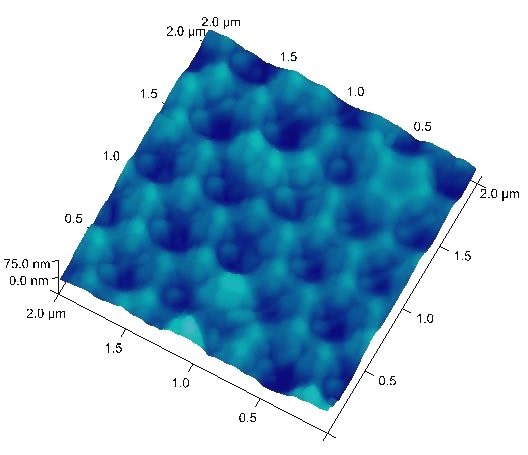
Typical anodization working ranges and the resulting pore-to-pore distances are 10-25 V and 35-70 nm for sulfuric acid, and 30-60 V and 80-150 nm for oxalic acid, respectively. These conditions are considered “mild anodization” and the AAO growth rate is relatively slow. Recently, the working ranges for oxalic acid has been extended to 120-150 V with the corresponding pore-to-pore distance expanded to 220-300 nm under the “hard anodization” condition.5 With a combined oxalic acid anodization followed by phosphoric acid anodization at 185 V, a pore-to-pore distance over 400 nm can be reached as shown in Figure 3.
In addition to large pore distance, another new direction in the synthesis of AAO films is to go beyond the 2D hexagonal pore arrays toward 3D periodically perforated nanostructure network.6 A cyclic anodization process was developed where an oscillatory current signal was applied to create AAO with pore diameter modulated by the applied current. The pore segments with larger diameter can be etched through to prepare periodically perforated nanopores. Another approach is to apply combined sequential mild anodization and hard anodization with pulsed anodization potentials.7 The result is a unique lamellar typed 3D structure. These novel nanostructures may open up possibility in molecular separation, photonic crystal, and solar cell applications.
AAO recent applications
Template based nanofabrication
AAO membranes have long been used for nanoscale fabrication. With one side of the membrane coated with a conductive material, electrodeposition can be carried out to deposit metallic nanowires, nanorods, or nanotubes, etc. Some examples include noble metals (Cu, Ag, Au),8,9 ferromagnets (Fe, Co, Ni),3 and conductive polymers (polythiophene, polyaniline, etc.10,11). Pd nanorods with 200 nm in diameter prepared from electrodeposition are shown in Figure 4. Electrodeposition is not limited to single component materials, more complex binary compounds such as semiconductive CdS, CdSe, and CdTe, have also been reported.12 An SEM image showing 200 nm PbSe nanorods are shown in Figure 5.
A broad range of ceramic metal oxide nanowires has been prepared with sol-gel infiltrated into AAO templates.13 In contrast to electrodeposition which usually carried out at ambient temperature, the sol-gel method requires high temperature calcination to form the metal oxides. AAO may not be inert at high temperature. Alumina template may also serve as a reactant to form a new template such as when ZnO is coated over AAO, in the presence of reducing hydrogen at high temperature, a new crystalline ZnAl2O4 nanotube network has been reported.14 Similar to sol-gel infiltration, polymer melt can be infiltrated into AAO template at temperature above 200 °C. After calcination above 600 °C, graphitic carbon nanotubes are formed inside of AAO template. Carbon nanotubes in AAO with pore widened to ~60 nm are indicated in Figure 6.15 Nearly aligned 200 nm carbon nanotubes with AAO template completely removed are shown in Figure 7.15 It is envisioned that these aligned carbon nanotubes may be filled with nanoparticles for magnetic alignment, drug delivery, thermal management applications.
With well controlled pulsed potential or current as well as the electrolyte concentration, multi-segmented nanowires have been reported. For examples, A/B segmented nanowires such as Co/Cu, Fe/Au, Ni/Au with segment length less than 100 nm have been prepared.16,17 The advantage for these nanowires is the tailoring of their intrinsic and geometric magnetic anisotropy. These new materials are designed for multifunction, controlled alignment, polarized spin injection for spintronics, magnetic switching through segment length, etc. This area is still very new and the choice of materials is strongly depending upon their compatible reduction potentials.
Improved energy efficiency
The preparation of the AAO template, it’s formation mechanism, and the synthesis of various nanowires and nanotubes have been discussed. Herein, selected AAO based energy related applications will be briefly reviewed. The AAO membrane with its well defined pore structure is an ideal platform for heterogeneous catalysis study.
The alumina surface has long been used in industry for catalyst support. The tunable pore diameter, pore-to-pore distance, and the pore depth allow one to control the surface area very well. Due to well defined surface area, the catalyst loading and the reactant exposure time can also be controlled. An AAO membrane with 40 nm pore diameter has been filled with alumina through atomic layer deposition (ALD) technique to reduce the pore diameter down to 10 nm (Figures 8, 9). 18,19 The ALD technique in contrast to chemical vapor deposition (CVD) allows sub-100 nm narrow pores to be filled one layer at a time. The coating is conformal and will not plug up the pore openings. We chose cyclohexane (C6H12) dehydrogenation reaction as a test and the goal is to selectively prepare cyclohexene (C6H10) but minimize the amount of benzene (C6H6).20 Conventional catalyst system will dehydrogenate cyclohexane all the way to benzene since it is a thermodynamically favored product. Comparing a V2O5 catalyst coated AAO membrane with 10 nm pore diameter with similar catalyst coating over alumina powders, we have indeed observed comparable amount of conversion but with significantly improved selectivity. The improved selectivity for the AAO catalysts may reflect a limiting of secondary oxidation reactions by a contact time of the reagents which is 103– 104 times shorter in the membrane channels than in the conventional catalyst bed.20 Therefore, the AAO membrane catalyst can improve the selectivity that leads to value added product.
The AAO template is playing a significant role in other energy related applications. All battery technologies are known to suffer from kinetic issues linked to the diffusion of Li in intercalation electrodes as well as the quality of the interfaces. Nanostructured electrodes are usually considered, however, the realization may not be straight forward. AAO template based nanofabrication provides a simple solution without using any expensive lithographic techniques. For example, AAO template was used to prepare a 200 nm Cu nanorod array onto a current collector. The AAO template was then removed. The exposed Cu nanorod surface was further coated with a polycrystalline magnetite (Fe3O4) thin film as a surface protection layer. The Fe3O4/Cu nanostructured electrodes demonstrated a factor of six improvement in power density over planar electrodes while maintaining the same total discharge time.21 There are numerous reports in the preparation of nanorod electrodes for Li battery application with use of AAO templates. In a related energy storage application, where excellent electrical property and high surface area of carbon nanotubes (CNTs) has attracted much attention as electrodes for supercapacitors, however, there is a large contact resistance between the electrodes and the current collector that limits their performance. AAO template was also used to provide a solution. A gold segment ~3 µm in length was first grown in a 60 µm AAO template. Multi-walled CNTs were then prepared over the Au segment through a CVD method. The CNTs/Au hybrid nanowires electrodes were verified to have low series resistance. A maximum power density of 48 KW/Kg was obtained at room temperature for a supercapacitor device with CNTs/Au electrodes. For a similar CNTs only device, a maximum power density of 18 KW/Kg was reported. The large improvement could be contributed to low contact resistance from the well adhered interfaces between CNTs and Au nanorod electrodes that were fabricated with the use of AAO templates.22 Toward the AAO based capacitors, very recently nanotubular metal- insulator-metal (TiN-Al2O3-TiN) devices prepared with AAO/ALD technique were reported to have a capacitance per unit planar area of ~10 µF/cm2 for 1-µm thick AAO and ~100 µF/cm2 for 10-µm thick AAO, significantly exceeding previously reported values for metal–insulator–metal capacitors in porous templates.23 In addition, the AAO template was recently applied to enhance the surface area of dye-sensitive solar cells (DSSC). The design was based on AAO membrane with 20 nm pore diameter and coated with a thin layer of ZnO with use of ALD technology. The reported result indicated photovoltage higher than those of other ZnO based DSSC, good fill factor, and a reasonable light-harvesting efficiency of 1.6%.24,25
Novel sensors for safety and security
AAO membranes are ideal substrates for various chemical and biochemical sensors for safety and security applications due to their tunable pore diameter, pore density, and high surface area. For example, we carried out first-step anodization to prepare a uniform AAO coating over Al surface. Upon removal of alumina, the Al surface was left with highly ordered nano-indents (Figure 2). These nano-indents serve as the nucleation sites for subsequent pore formation. Brief second-step anodization was performed with time increments between 2 and 12 minutes, these well-defined surfaces with nanowells in different depths can be used for sensor substrates. When coated with a Pd thin film of less than 10 nm, the Pd formed weakly connected islands over the AAO substrate and showed chemo-resistive behavior toward hydrogen gas under Ar and air.
As shown in Figure 10, the resistance as a function of hydrogen input is plotted with time and the AAO/Pd surface (400×400 nm AFM image) is also shown in the insert. The sensitivity (.R/R0) is plotted versus the square root of hydrogen concentration in Figure 11 and the linear behavior serves as the basis for hydrogen sensing.26
Sub-micron metallic barcode nanowires such as Au-Ag-Au, Au-Ag-Ni-Pd-Pt, etc… were prepared by sequential electrochemical deposition of metal ions into templates with uniformly sized pores. The differential reflectivity of adjacent stripes enables identification of the striping patterns by conventional light microscopy. Metal surface derivatization allows different segments to be labeled for fluorescence imaging and such readout mechanism allows DNA and protein bioassays.27 The segment length has been reduced to tens of nm to create “on-wire” lithography.28 Magnetic memory devices have been developed (section 4.1).16,17 When segments are combined metal- polymer such as Au-polypyrrole, curved superstructures can be formed through self- assembly, and actuation can be induced by humidity, temperature, and light.29 More applications in superconductivity, optical microscopy and sensing, as well as mechanical energy from template grown nanowires have been reviewed.30
Due to optical interference, thin nanoporous alumina film over aluminum may give rise to interference colors (Figure 12). The colors can be controlled through thin film thickness, porosity, intrinsic nanostructures, and viewing angle, etc. In contrast to organic dye based colors, the nanostructure based interference colors will not suffer from fading, chemical decay, etc. We found that interference colors can be strongly enhanced with small amount of metal coating such as Ag, Au, Pd, etc. (Figure 12).31 It is envisioned that when AAO nanowells surface is derivatized, an interference color sensor can be developed. Toward that goal, we functionalized the alumina surface with 3-amino-propyl-trimethoxysilane (APTS). APTS is designed to form complexes with nitroaromatics, a typical component for explosives. Each interference color gives rise to an oscillation pattern through UV-Vis reflectance measurement. We compare the as prepared AAO nanowell (black trace, bottom), AAO with APTS coating (red trace, top) and AAO with APTS exposed to trinitrotoluene (TNT) solution (Figure 13). Our preliminary results indicated that reflectance spectra shift toward longer wavelength in the following order: AAO, AAO/APTS, AAO/APTS/TNT. The results are consistent with the surface coating thickness is increasing following the same order, therefore, the AAO nanowells can be used to develop a chemical sensor.
AAO membranes with unique intrinsic 3D nanostructures have also been reported to demonstrate photonic band gap in the visible region. The band gap is tunable through chemical etching. This photonic crystal behavior may be used for narrow band filters in diffractive optics application.32 A typical limitation during photo- and e-beam lithography is the isotropic etching. During chemical etching of Si, the etched area tends to go beyond the patterned area to generate slanted side walls. The AAO membranes due to their intrinsic nanopores with very high aspect ratio (over 1,000) have recently been applied as new materials for micro-electro-mechanical systems (MEMS) application. AAO-based sensors are proven to be highly sensitive for ambient relative humidity changes. An AAO-based humidity sensor has been incorporated into an integrated circuit so that developed wireless sensor network can be readily applied.33 AAO based device has been tested for radio frequency MEMS inductor.34 In addition, AAO membrane has been fabricate into micro-cantilever for AFM and for chemical sensing applications.35
There is a new effort in developing AAO membrane into a Multi-channel plate (MCP) detector. A MCP is a planar component used for detection of particles (electrons or ions) and impinging radiation (ultraviolet radiation and X-rays). It is closely related to an electron multiplier, as both intensify single particles or photons by the multiplication of electrons via secondary emission. MCP is an array of micropores imbedded in a lead silicate glass. The surface is treated with proper chemicals to enhance the secondary electron emission.36 Typical commercially available MCP is built with channel diameter between 10 and 25 microns, and micropore length to diameter ratio between 40 and 100.
The channel diameter is known to affect three important aspects of a detector. Firstly the temporal response of the device is determined by the pore size and smaller pore size makes faster time response. This is important for ultrafast measurements. Secondly, the spatial resolution that is the capability to differentiate two stationary point sources, and smaller pore improves this imaging resolution. Thirdly, the smaller pore recharges faster than that of the larger pores and the device dead time is reduced. Therefore, smaller pore diameter is preferred and the current sate-of-the-art MCP is developed with 2.3 micron pore diameter.37
The lead glass MCP is fabricated through a multi-step process starting with melting of new glass materials, fiber draw, slicing, polishing, and chemical processing.37 It is elaborate, expensive, difficult to further reduce the channel diameter, and very hard to scale up for large area detection applications. The state-of-the-art MCP with 2.3 microns pore size is shown in Figure 14 and an AAO template with 80 nm pore diameter and 145 nm pore-to-pore distance is shown in Figure 15. Both MCP and AAO show similar hexagonally closed packed pattern. Since the AAO pore diameter (30 to 300 nm) and pore-to-pore distance are highly tunable, AAO pores are much smaller than that of the conventional lead glass, and AAO can be prepared in a simple wet chemistry lab, AAO has attracted significant interest recently as a candidate for new MCP design and development.
However, there is a significant challenge to synthesize AAO membranes with targeted 2 microns pore diameter. At present, the largest AAO pore diameter with good order is ~0.3 micron which is about one order of magnitude smaller than that of the MCP.
AAO holds the promise of highly scalable which is required for large area detector as well as relatively inexpensive. Various lithographic techniques are being explored to pattern the Al surface before anodization.38 It remains to be seen whether AAO with large pores (> 1 µm) can be synthesized as well as stabilized.
Summary
In this article, the synthesis, formation mechanism, and new 3D nanostructures of anodized aluminum oxide (AAO) are briefly discussed. The use of the AAO as a template for nanofabrication and the membrane itself has been reviewed. Many new and potential applications in improved energy efficiency as well as for safety and security are summarized. Certainly the review is not comprehensive. Novel use of the AAO template is an on-going effort in the research community as evident by the increasing AAO related publications in recent years. Some of these new applications will most likely make into the market place in the near future.
Acknowledgments Argonne National Laboratory's work was supported by the U. S. Department of Energy, Office of Science, Office of Basic Energy Sciences, under contract DE-AC0206CH11357.
References
(1) Keller, F.; Hunter, M. S.; Robinson, D. L. J. Electrochem. Soc. 1953, 100, 411.
(2) O'Sullivan, J. P.; Wood, G. C. Proc. Roy. Soc. Lond. A 1970, 317, 511.
(3) Wang, H. H.; Han, C. Y.; Willing, G. A.; Xiao, Z. Mat. Res. Soc. Symp. Proc.
2003, 775, 107-112.
(4) Masuda, H.; Satoh, M. Jpn. J. Appl. Phys. 1996, 35, L126-L129.
(5) Lee, W.; Ji, R.; Gösele, U.; Nielsch, K. Nature Materials 2006, 5, 741-747.
(6) Losic, D.; Losic Jr., D. Langmuir 2009, 25, 5426–5431.
(7) Lee, W.; Schwirn, K.; Steinhart, M.; Pippel, E.; Scholz, R.; Gösele, U. Nature Nanotechnology 2008, 3, 234-239.
(8) Foss Jr., C. A.; Tierney, M. J.; Martin, C. R. J. Phys. Chem. 1992, 96, 9001-9007.
(9) Masuda, H.; Fukuda, K. Science 1995, 268, 1466.
(10) Fu, M.; Zhu, Y.; Tan, R.; Shi, G. Adv. Mater. 2001, 13, 1874-1877.
(11) Xiong, S.; Wang, Q.; Xia, H. Materials Research Bulletin 2004, 39, 1569–1580.
(12) Xu, D.; Chen, D.; Xu, Y.; Shi, X.; Guo, G.; Gui, L.; Tang, Y. Pure Appl. Chem.
2000, 72, 127–135.
(13) Shankar, K. S.; Raychaudhuri, A. K. Materials Science and Engineering 2005, C25, 738 – 751.
(14) Wang, Y.; Wu, K. J. Amer. Chem. Soc. 2005, 127, 9686-9687.
(15) Han, C. Y.; Xiao, Z.-L.; Wang, H. H.; Lin, X.-M.; Trasobares, S.; Cook, R. E. J.
Nanomaterials 2009, Article ID 562376.
(16) Clime, L.; Zhao, S. Y.; Chen, P.; Normandin, F.; Roberge, H.; Veres, T.
Nanotechnology 2007, 18, 435709.
(17) Lee, J. H.; Wu, J. H.; Liu, H. L.; Cho, J. U.; Cho, M. K.; An, B. H.; Min, J. H.; Noh, S. J.; Kim, Y. K. Angewandte Chemie International Edition 2007, 46, 36633667.
(18) Pellin, M. J.; Stair, P. C.; Xiong, G.; Elam, J. W.; Birrell, J.; Curtiss, L.; George, S.
M.; Han, C. Y.; Iton, L.; Kung, H.; Kung, M.; Wang, H. H. Catalysis Letters 2005, 102, 127-130.
(19) Elam, J. W.; Xiong, G.; Han, C. Y.; Wang, H. H.; Birrell, J. P.; Welp, U.; Hryn, J.
N.; Pellin, M. J.; Baumann, T. F.; Poco, J. F.; Satcher Jr., J. H. Journal of Nanomaterials 2006, Article ID 64501.
(20) Stair, P. C.; Marshall, C.; Xiong, G.; Feng, H.; Pellin, M. J.; Elam, J. W.; Curtiss, L.; Iton, L.; Kung, H.; Kung, M.; Wang, H. H. Topics in Catalysis 2006, 39, 181186.
(21) Taberna, P. L.; Mitra, S.; Poizot, P.; Simon, P.; Tarascon, J.-M. Nature Materials 2006, 5, 567-573.
(22) Shaijumon, M. M.; Ou, F. S.; Ci, L.; Ajayan, P. M. Chem. Commun. 2008, 2373– 2375.
(23) Banerjee, P.; Perez, I.; Henn-Lecordier, L.; Lee, S. B.; Rubloff, G. W. Nature Nanotechnology 2009, 4, 292-296.
(24) Martinson, A. B. F.; Elam, J. W.; Hupp, J. T.; Pellin, M. J. Nano Lett 2007, 7, 2183-2187.
(25) Martinson, A. B. F.; Elam, J. W.; Liu, J.; Pellin, M. J.; Marks, T. J.; Hupp, J. T.
Nano Lett 2008, 8, 2862-2866.
(26) Rumiche, F.; Wang, H. H.; Hu, W. S.; Indacochea, J. E.; Wang, M. L. Sensors and Actuators B 2008, 134, 869–877.
(27) Nicewarner-Peña, S. R.; Freeman, R. G.; Reiss, B. D.; He, L.; Peña, D. J.; Walton, I. D.; Cromer, R.; Keating, C. D.; Natan, M. J. Science 2001, 294, 137-141.
(28) Qin, L.; Park, S.; Huang, L.; Mirkin, C. A. Science 2005, 309, 113-115.
(29) Lim, J. K.; Ciszek, J. W.; Huo, F.; Jang, J.-W.; Hwang, S.; Mirkin, C. A. Nano Lett 2008, 8, 4441-4445.
(30) Kline, T. R.; Tian, M.; Wang, J.; Sen, A.; Chan, M. W. H.; Mallouk, T. E. Inorg.
Chem. 2006, 45, 7555-7565.
(31) Wang, H. H.; Son, K.-I.; Lee, B.; Lu, J.; Han, C. Mater. Res. Soc. Symp. Proc.
2007, 951, 0951-E09-10.
(32) Wang, B.; Fei, G. T.; Wang, M.; Kong, M. G.; Zhang, L. D. Nanotechnology 2007, 18, 365601.
(33) Juhász, L.; Vass-Várnai, A.; Timár-Horváth, V.; Desmulliez, M. P. Y.; Dhariwal, R. S. In Design, Test, Integration & Packaging of MEMS/MOEMS French Riviera, , 2008.
(34) Oogarah, T. B., Master Thesis, Elec. and Comp. Eng., the University of Waterloo, 2008.
(35) Lee, P.-S.; Lee, J.; Shin, N.; Lee, K.-H.; Lee, D.; Jeon, S.; Choi, D.; Hwang, W.; Park, H. Adv. Mater. 2008, 20, 1732 - 1737 (36) Wiza, J. L. Nuclear Instruments and Methods 1979, 162, 587-601.
(37) Laprade, B.; Starcher, R., http://www.burle.com/cgibin/ byteserver.pl/pdf/2micron2.pdf 2001.
(38) Drobychev, G.; Barysevich, A.; Delendik, K.; Karneyeu, A.; Nédélec, P.; Sillou, D.; Voitik, O. Nuclear Instruments and Methods in Physics Research A 2006, 567, 290–293.
RELATED CONTENT
-
Preventing Anodizing Cathodes from Turning Red
While the red color may not be desirable, anodizing expert Drew Nosti says it poses no particular problem to a successful anodizing process.
-
Deoxidizing Aluminum as a Pretreatment
This important first step can help prepare the metal for subsequent surface finishing.
-
Plating Q&A: Can you color stainless steel?
Our expert, Art Kushner, says yes, you can color stainless steel, but it is not a process that is typically performed in a plating shop. Read more about his answer.


