Thin Multilayer Palladium Coatings for Semiconductor Packaging Applications Part I: Solderability
The 1996 AES Gold Medal Award was given to I.V. Kadija and his co-workers for the Best Paper appearing in Plating and Surface Finishing in 1995. Their work dealt with the use of palladium in electronics finishing in the 1990s. This paper covered the evaluation of such finishes for solderability.
#research #electronics
by
I.V. Kadija, J.A. Abys, J.J. Maisano, E.J. Kudrak and S. Shimada
Featured Content
Editor’s Note: Originally published as I.V. Kadija, et al., Plating and Surface Finishing, 82 (2), 56-62 (1995), and was awarded the 1996 AES Gold Medal for Best Paper published in Plating and Surface Finishing in 1995. A printable PDF version is available by clicking HERE.
ABSTRACT
A study of the physical and chemical characteristics of electroplated palladium has led to an understanding of its performance as a solderable and wirebondable material. Investigation of the interactions of porosity, interdiffusion, oxidation and dissolution rates of various metals in Sn-Pb solder has led to the design of various multilayered palladium coatings useful for advanced electronic packaging applications. Combinations of palladium and palladium alloys with a thin gold flash exhibit good solderability and wirebonding performance and meet the stringent requirements of MIL-STD-883, Methods 2003 and 2022.
Introduction
Packaging is a critical operation in integrated circuit (IC) device fabrication. Compact devices, such as multi-chip-modules (MCMs), are being produced with greater functionality and contact density; this has increased process complexity, quality, yield requirements and cost.1-3 The yield, and thus the cost of packaging operations is dependent on the performance of processes such as soldering, wirebonding, and encapsulation, which in turn are highly dependent on the type and quality of the lead-frame surface finish. Conventional lead-frame finishes, such as the Ag Spot/Sn-Pb finish, utilize multi-step, selective plating operations and require the use of expensive "step & repeat" selective spot plating equipment. Moreover, in the case of the pre-plated Sn-Pb solder finish (Fig. 1), the following problems may arise:4,5
- Silver migration
- Solder bridging (especially for fine-pitch packages)
- Incompatibility with packaging operations
- Shortened shelf-life
- Lack of control of solder thickness (hot solder dip process)
Alternatively, a post-plating Sn-Pb process (Fig. 1), may suffer from one or more of the following:
- Silver migration
- Solder bridging
- Exposure of IC package to corrosive plating chemicals
- Incompatibility of final packaging operation with Sn-Pb
- Shortened shelf-life

Figure 1 - Lead-frame metal finishing packaging process choices.
The semiconductor packaging industry would like to utilize a universal finish that would be solderable and wirebondable, regardless of process exposure or shelf-life requirements,4,5 and overcome shortcomings of the current processes. Because a typical packaging sequence, as shown in Fig. 2, may expose the materials involved to extreme conditions, resulting in base metal oxidation, interdiffusion, contamination and mechanical stress, any new process must meet stringent reliability requirements.
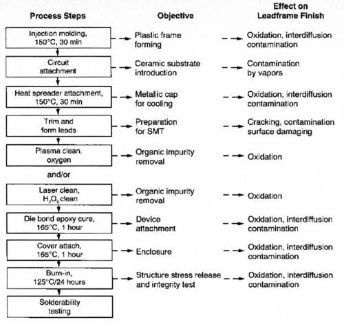
Figure 2 - Typical advanced IC packaging process.
D.C. Abbott, et al., of Texas Instruments, have pioneered a palladium-plated lead-frame process and have discussed its positive impact on component reliability and quality.5,6 The focus of their development was a "universal" lead-frame finish that reduced process complexity, increased yields and presumably lowered the overall cost for IC packaging operations. According to Abbott, et al., the use of palladium as an overall finish accomplishes these objectives and has several advantages from a plating perspective.6 The elimination of silver cyanide from the process makes it inherently safer and reduces waste treatment costs. Because palladium is plated over the entire surface, the design, construction and operation of the plating line is simplified, further reducing costs. In addition, product changeovers are simple, requiring no line or tooling changes, which significantly reduces downtime. The use of palladium as an overall finish is not without controversy, however. For example, one commercially available palladium finish focuses on the use of a scheme to protect the substrate material (e.g., Cu, Cu-alloy, Alloy 42) from oxidation and interdiffusion, which may interfere with packaging performance. In this case, a very thin, single layer of palladium (~3-5 μ-in.) is utilized as a "protective" and "sacrificial" thin film, which dissolves in the Sn-Pb solder and allows a bond to form to an oxide-free, uncontaminated nickel sublayer. Depending on the application and specific performance requirements, this approach could be problematic.
The focus of this work has been to understand the physical and chemical characteristics of electroplated palladium and the relationship of deposited layer structures to porosity, interdiffusion, oxidation and rates of dissolution in solder. One specific aim was to develop a cost-effective pre-plated lead-frame process,7 compatible with existing packaging operations and that meets the stringent solderability requirements of MIL-STD-883, Methods 2003, 2022, thermal aging criteria, which are specific to individual packaging operations, and the AT&T wirebonding specification A-87 AL1917. Our efforts resulted in the development of a multi-layered system (MLS) meeting these specifications. The MLS consists of one to three layers of palladium and palladium-alloys with or without a gold flash, depending on specific performance requirements. This report will consider solderability data only; wirebonding details will follow in a subsequent report.
Experimental procedure
Surface finish sample matrix
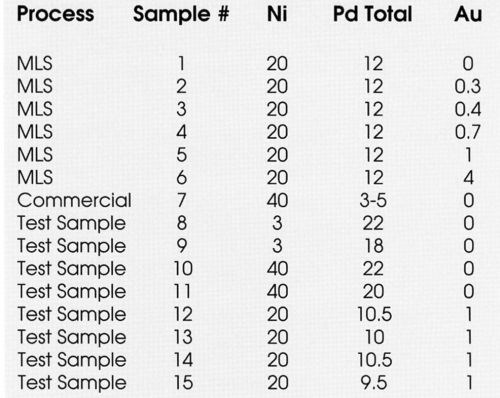
It has been established that relatively thick (>20 μ-in.) gold-flashed palladium (GFPd) can provide excellent solderability and wirebondability.4 Because of the high thicknesses of precious metal layers,4 the cost has been considered prohibitive by manufacturers of integrated circuits. For this purpose, thinner (<15 μ-in.) multilayer finishes were investigated, as shown in Table 1.
Table 1 - Substrates by layer configuration and thickness, μ-in.
Solderability standard test
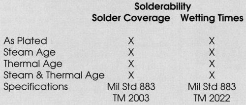
Various standardized tests were undertaken to evaluate the solderability of the above finishes, as shown in Table 2. Samples 1 through 7 were evaluated through this matrix of tests. The selected standard test for solder coverage was MIL-STD-883, TM 2003, which entails exposure of the plated finish to 95°C and 95% relative humidity (RH), followed by a "dip and look" inspection procedure for non-wetted or de-wetted areas and/or surface irregularities. Immersion in the solder pot was accomplished by means of a mechanical dipping device, as specified in MIL-STD-202F, TM 208F. Moreover, it is also critical that soldering is achieved within one second to be compatible with the line speed of current packaging operations. TM 2022, the wetting balance test, was utilized to determine wetting speed of the above finishes.
Table 2 - Matrix of tests.
Exposure of a lead-frame to high temperatures for prolonged periods of time causes interdiffusion of the metals and could change the surface composition. If, during this process, a "non-noble" metal is transported to the surface and oxidizes, the solderability performance is adversely affected. Thus, thermal aging is utilized to evaluate lead-frame finishes. We selected 150, 200 and 250°C for 1-, 2-, and 5-hr exposures as typical thermal aging parameters.
Porosity, diffusivity and oxidation
Samples 8 through 15 were prepared to examine the effect of porosity on solderability, as-plated, and after steam aging. The standard porosity test utilized was ASTM B 799-88: "Sulfurous Acid Vapor Porosity Testing." Its significance will be discussed in a later section. Auger electron spectroscopy (AES) surface analysis and depth profiling were implemented in the investigation of thermal aging and interdiffusion phenomena.
Results
Solder coverage
One of the objectives of this development was to evaluate a commercially available finish (Table 1, Sample 7) and determine its performance relative to our proprietary multilayer finishes. The performance of the commercial finish is summarized in Figs. 3-5 and compared with several MLS finishes in Table 3. This system does not meet the criteria of MIL-STD-883, 2003/2022. Further, its performance deteriorates catastrophically under thermal aging conditions.
Table 3 - Solderability results.

Figure 3 shows that the steam aging test of the "commercial" finish (Sample 7) exhibits gross solderability failures and gross porosity to the nickel surface. The relationship between porosity and solderability will be elucidated in the next section. Figures 4 and 5 examine the thermal aging properties of the commercial finish at 200 and 250°C. Under both conditions, it is clear that nickel and other contaminants have diffused to the surface and that performance deteriorates to unacceptable levels. Auger data indicates that the presence of 2-3% (atomic) nickel is enough to cause deterioration of the solderability. Overall, these data suggest that the palladium layer thickness of the commercial sample is too thin and too porous to protect the nickel substrate from oxidation and other contaminants from diffusing to the surface, thus compromising solderability.
Alternatively, Samples 1 and 2, the MLS without gold or with an ultra-thin (0.3 μ-in.) gold flash, also do not meet the 8-hr steam aging test, but are able to pass 150 and 200°C thermal aging. Sample 3, which is the MLS with -0.4 μ-in. of gold, passes the steam and thermal aging tests up to 200°C. Samples 4-6 will pass the steam and thermal aging tests up to 250°C for 5 hr, but only Samples 5 and 6, with a gold flash >1 μ-in., pass thermal aging for 5 hr, followed by 8-hr steam aging.
These data indicate that to pass the 8-hr steam aging test consistently, it is desirable to utilize ~0.5 μ-in. of gold on the palladium MLS finishes. It also clearly demonstrates the superior performance of a multi-layered structure when the objective is the minimization of non-noble metals at the surface.
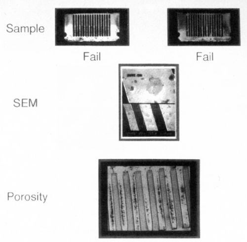
Figure 3 - Solderability of commercial palladium finish - steam aging effect.
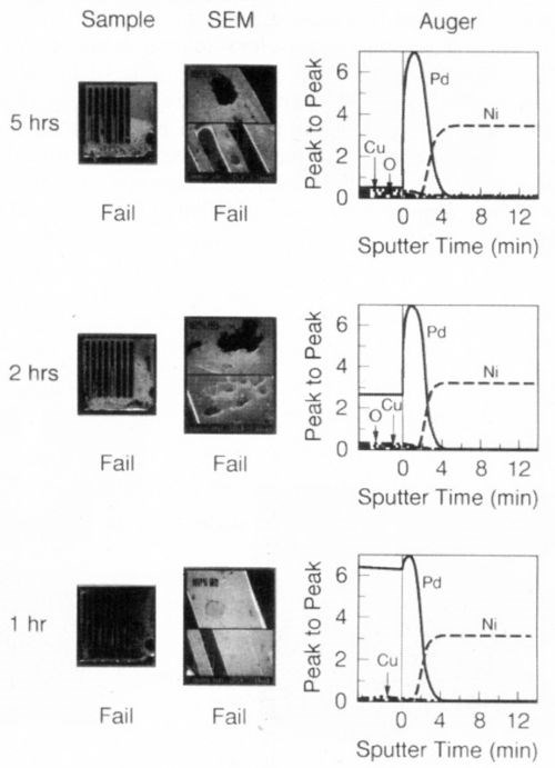
Figure 4 - Solderability of commercial palladium finish - thermal aging effect at 200°C.
Porosity vs. solderability performance
Porosity to the substrate or basis metal contributes to surface finish degradation. This is a well-studied phenomenon in connector reliability, where migration and oxidation or corrosion of substrate metals lead to surface contamination and a subsequent increase in contact resistance.8-11 As suspected, this mechanism may significantly contribute to poor solderability. A schematic representation of this phenomenon, as seen in Fig. 6, attempts to demonstrate that the presence of pores is a conduit for the interaction of the environment with the base metal and/or substrate metal layer.
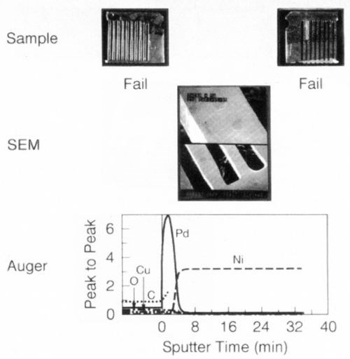
Figure 5 - Solderability of commercial palladium finish - thermal aging effect at 200°C for 10 hr followed by steam aging.
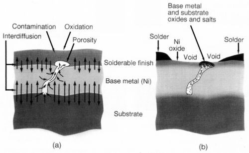
Figure 6 - Substrate/solder interface schematic representation.
Figure 7 illustrates a sample plated under conditions that resulted in gross porosity. As can be seen, the solderability of the as-plated sample is acceptable. After steam aging, however, the solderability deteriorates to unacceptable levels. The sulfurous acid vapor test demonstrates the presence of gross porosity to the nickel substrate, as shown in the 10× optical photograph. This porosity indicates the presence of exposed nickel, which is attacked by the SO2 vapor. Thus, it is reasonable to conclude that, when exposed to the steam aging test, or exposed to the ambient during storage, a nickel oxide film would form and compromise solderability.
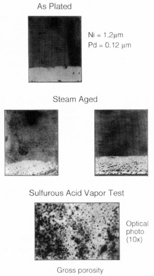
Figure 7 - Thin palladium over nickel: porosity effect on solderability.
To investigate further the possible correlation between porosity and solder coverage, a series of samples was prepared with varying degrees of porosity by manipulating plating variables (Table 1, Samples 8-15). Table 4 summarizes the results. As can be seen, the pores vary from ~11 pores/cm2 to >100 pores/cm2 and in the as-plated condition, the solderability is acceptable for all samples. After steam aging, however, the samples with >100 pores/cm2 showed unacceptable (< 95%) solderability.
Table 4 - Porosity vs. solderability.
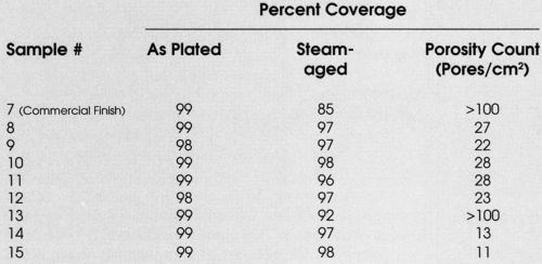
This relationship between porosity and solderability after steam aging is demonstrated more pointedly in Figs. 8 and 9. In Samples 12-15, the palladium thickness was fixed at ~10 μ-in., with a nominal one μ-in. gold cap to demonstrate that total thickness is not necessarily the only parameter of importance. Low porosity levels (<25 pores/cm2) are desired to obtain acceptable solderability after steam aging; however, this phenomenon has not been quantified.
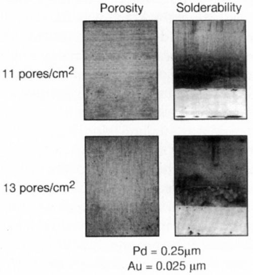
Figure 8 - Gold-flashed palladium: porosity effect on solderability.

Figure 9 - Gold-flashed palladium: porosity effect on solderability.
Interdiffusion of metals vs. solderability
The interdiffusion of metals must be considered when developing a finish for lead-frame applications because of the high processing temperatures (>150°C) and exposure times experienced in packaging operations. The specific rate of diffusion and extent of interdiffusion are functions of the metals employed, the nature of the electrodeposited structure, the layering and thickness of the metals, the temperature and the exposure times.12,13 Obviously, interdiffusion will be more pronounced at higher temperatures and prolonged exposure times.
As discussed in the previous sections, the presence of exposed nickel or other basis metal oxides will cause solder ability failures. It is also likely that thin single layers (<0.25 μ-in.) of palladium will be insufficient to completely prevent thermal diffusion of basis metals to the surface. Thus, the thickness and layered structure of the palladium is relevant, not only from a perspective of reduced porosity, but as a thermal diffusion barrier as well.
A simple experiment was undertaken to demonstrate the relative performance of gold and palladium in inhibiting diffusion of nickel. Gold or palladium was plated to a thickness of 0.6 μm over 1.2 μm of nickel. The samples were aged at 250°C for 1, 5 and 10 hr (Fig. 10). Within one hr of aging, the soft gold lost its solderability, whereas the palladium survived 5 hr under these conditions. An Auger surface scan, Fig. 11, of the 10-hr palladium sample, clearly shows the presence of nickel on its surface; nickel was absent on the 5-hr sample. These findings support the role of nickel diffusion and oxidation and its deleterious effect on solderability.
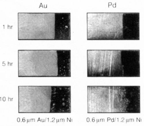
Figure 10 - Solderability comparison: Soft gold vs. palladium - interdiffusion phenomenon.
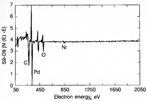
Figure 11 - Surface survey by Auger, thermally aged Pd, 5 hr, 250°C.
To optimize the MLS finish further, we applied the principle of alloying layers.12 Figure 12 shows an Auger depth profile of two finishes, Samples 1 and 5. By depositing ~1 μ-in. of gold on the palladium, the diffusion of nickel was further inhibited, as observed by its absence at the surface. This dramatically improves its solderability and enhances wetting speed, as discussed in the next two sections.
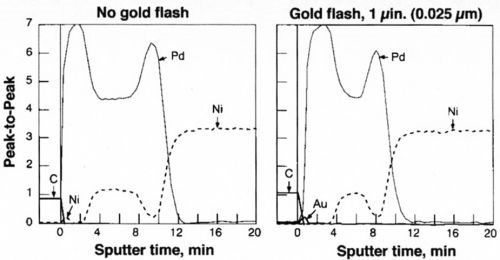
Figure 12 - Auger depth profiles of MLS vs. gold flashed MLS finishes.
Intrinsic oxides and dissolution rates of surface layers - effect on solderability
Although noble metals are considered non-oxidizing, it has been established that thin layers of oxide or chemisorbed oxygen form on their surfaces.14-16 The tenacity of these surface oxides varies among the noble metals. Table 5 shows the standard molal enthalpies of the oxides of gold, platinum, palladium, nickel and tin, along with their solderability.
Table 5 - Oxide formation thermodynamics vs. solderability.

Gold promptly forms oxygen monolayers in air, but its oxides are unstable and a positive molal enthalpy indicates that its natural state is oxide-free.16 Additionally, gold readily dissolves in tin-lead solder to form various intermetallic gold alloys.13 These characteristics are two of the reasons why the gold-flashed MLS lead-frames exhibit excellent solderability. Table 5 further indicates that the oxidation thermodynamics and the dissolution rates cannot be the only factors used to predict solderability performance. For example, some noble metals, such as platinum, are almost oxide-free in their natural state; yet, platinum, which has a positive enthalpy for one oxide, PtO2, and a small negative enthalpy for Pt3O4, is entirely non-wettable. A different process may be responsible for this behavior. Bader shows that the platinum dissolution rate is more than 108 times slower than that of gold;13 thus, the formation of intermetallic bond is probably inhibited because of the extremely slow dissolution of platinum in solder.
The behavior of nickel and tin oxides reveals another interesting phenomenon. Tin oxide is more stable than nickel oxide; yet, tin oxide, which is ubiquitous in tin-lead films, does not inhibit solderability, while nickel oxide has a recognized deleterious effect. This may be explained by the fact that the tin-lead beneath its native oxide melts during soldering, fracturing and dispersing the relatively thin oxide layer in the pool of molten solder. This cannot occur with nickel because the melting points of nickel and its oxide are relatively high.
Palladium forms a weak oxide in air, as indicated by the enthalpy. This, coupled with an acceptable dissolution rate, shows good to marginal solderability.
Wetting time
The wetting speed of a particular electroplated finish in solder is dependent not only on the intrinsic dissolution rate of the metals, but also on deposit film characteristics, such as porosity, interdiffusion, contamination and oxidation. As established earlier, the commercial finish (Sample 7) is inferior to the MLS finishes in meeting steam and thermal aging with respect to solderability requirements. Thus, it may be concluded that the presence of nickel oxides, as discussed previously, would also degrade wetting speed.
The results in Table 6 demonstrate this by showing that for Sample 7 only the as-plated condition has a wetting time of less than one second. Sample 1, on the other hand, shows similar wetting times in the as-plated condition, but relatively lower times in the steam and thermally aged samples. Sample 1 has a relatively thicker (12 μ-in.) MLS finish without a gold flash; it has been shown to be less porous and a better diffusion barrier than the commercial finish. Alternatively, if lower wetting time is required in the aged condition, the presence of a gold flash accomplishes this objective. Inasmuch as gold dissolves in solder at significantly higher rates (Table 5) and inhibits the diffusion of non-noble metals, it may be presumed that its presence or, for that matter, a Au-Pd alloy surface could wet much faster than pure palladium. The data in Table 6 seem to support this hypothesis.
Table 6 - Wetting time vs. aging.

Soldered bond strength
As part of an evaluation of surface mount technology applications, a series of pull tests was performed on solder bonds formed with multi-chip modules. The leads and substrates were prepared with palladium multilayer finishes and subsequently soldered in a surface-mount processing operation. The leads were cut from the device and individually tested for pull force until breakage occurred. In Fig. 13, the pull strength is compared for three finishes - multilayer Pd, Sn-Pb/Cu and Sn-Pb/Ni. The mean bond strengths are: 2.62 lb. for multilayer Pd, 2.09 lb. for Sn-Pb/Cu, and 1.78 lbs. for Sn-Pb/Ni. These tests show that palladium finishes are superior in bond strength, providing an additional advantage to the devices utilizing this finish.
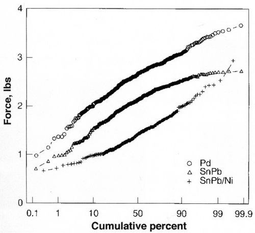
Figure 13 - Bond strengths of solder joint: Pd MLS vs. Sn-Pb.
Conclusions
Palladium and palladium-alloy electrodeposits can be effectively utilized in metal finishing for electronics packaging applications. By combining layers designed to preserve the integrity of the surface finish by limiting porosity, inhibiting thermal diffusion, and increasing wetting speeds, the most stringent soldering requirements have been met. A summary of these data and a comparison with Sn-Pb coatings is shown in Fig. 14.
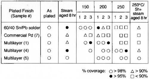
Figure 14 - Solderability of palladium finishes after thermal and steam aging.
References
1. C. Bolch and J. Ranghanatan, Proc. Symp. Electronic Mfg. Technol., IEEE/CHMT 11th Int'l Conf. (1991).
2. J. Hodson, Electronic Packaging and Production, 32 (10), 34 (1992).
3. R.R. Tummala and E.J. Rymaszewaki, Microelectronics Packaging Handbook, Van Nostrand Reinhold, New York, NY, 1992.
4. I.V. Kadija, J.A. Abys, E.J. Kudrak and J.J. Maisano, Proc. AESF SUR/FIN '92, Session F (1992).
5. D.C. Abbott, M. Mitchell and B. Lockhorst, Proc. EAST Conf., Schwäbisch Gmünd, Germany (Nov., 1991).
6. D.C. Abbott, R.M. Brock, N. McLelland and J.S. Wilty, IEEE Trans. on Components, Hybrids and Mfg. Technol., 14 (3), Sept., 1991.
7. J.A. Abys, I.V. Kadija, E.J. Kudrak and J.J. Maisano, U.S. patent 5,360,991 (1994). Japanese Patent Application, H06-196305, filed July 29, 1994.
8. M. Clarke, "Porosity and Porosity Tests," in Properties of Electrodeposits, Sard, Leidheiser and Ogburn, eds., The Electrochem. Soc, 122, Princeton, NJ, 1975.
9. S.J. Krumbein, Trans. Symp. Connector and Interconn. Technol., Philadelphia, PA, 47 (Oct., 1987).
10. E.J. Kudrak and J. A. Abys, Interconnection Technol., 9, 18 (June, 1993).
11. E.J. Kudrak, et al., Plating & Surface Finishing, 79 (2), 49 (1992).
12. CD. Iacovangelo, Proc. AESF SUR/FIN '92, Session J (1992).
13. W.G. Bader, Proc. AESF Symp. on Economic Use of & Substitution for Precious Metals in the Electronics Industry; Danvers, MA (Sept., 1980); W.G. Bader, Welding Journal Research Supplement, p. 1-7, (Dec., 1969).
14. M. Tandy and F. Bozon-Verduraz, Compt. Rend., C 280, 317 (1975).
15. Lange's Handbook of Chemistry, McGraw-Hill Book Co., New York, NY; Gmelins Handbuch Der Anorganishen Chemie, Gold, 62, Verlag Chemie, GmbH, Weinheim/Bergenstrasse, 1954.
16. J.E. Brady and G.E. Humiston, General Chemistry, J. Wiley & Sons, New York, NY, 1978.
About the authors


RELATED CONTENT
-
History of Chromium Plating
A review article originally printed as Plating & Surface Finishing, 71 (6), 84-91 (1984) on the occasion of the 75th anniversary of the founding of the American Electroplaters Society.
-
Black Chromium Finishing: Beauty and the Beast
Over the past 10 years, there has been commercial development of black chromium deposits from a trivalent chromium electrolyte. This paper will review the deposit characteristics and operational consideration of these similar, but different chromium plating deposits.
-
Special Aspects of Electrodeposition on Zinc Die Castings
Electroplating is a frequent choice to give zinc die cast components a high-quality protective and decorative surface finish, however, applying this kind of treatment for die cast zinc components presents hidden challenges. In order to overcome these issues, a thorough morphology and composition analysis of die cast items was conducted. Special aspects of zinc die cast as a plating substrate are described and linked to the die casting process.


