This overview takes a look at vacuum deposition technologies as processes that may be used to create coatings that can be substituted for or enhances the properties of electroplated coatings. Initially, this work discusses trends in metal finishing and environmental regulation.
The product finisher is facing many challenges as the overall coating industry is changing with increased regulations, competition and performance requirements. This overview takes a look at vacuum deposition technologies as processes that may be used to create coatings that can be substituted for or enhances the properties of electroplated coatings. Initially, this work discusses trends in metal finishing and environmental regulation. It covers some recent rulings on the use of hexavalent chromium, which is driving the electroplating industry to look at new chemistries and new processes like vacuum coating. This study provides an overview of a range of physical vapor deposition (PVD) and some chemical vapor deposition (CVD) coating technologies. Some notable finishing companies such as Kohler have embraced vacuum coating as a technique to make a better product.
Many finishers are looking at new coating processes that may be more environmentally friendly or more economical. New processes called “dry” processes such as vacuum deposition are being seriously considered since they involve no aqueous component of the deposition process. Another trend is the move away from metals to non-metallic surfaces, such as plastics and composites to be coated. The industry sees strong trends towards non-metallics in the automotive, aerospace and electronics industries. Some finishers have even moved processing out of the US to facilities in Mexico and Asia where environmental constraints are less stringent. Fig. 1 shows the results of a National Metal Finishing Resource Center (NMFRC) survey showing the 9 top industry trends and how they are driven by a combination of regulatory, technology and economic drivers.In many cases the Return on Investment (ROI) is the controlling factor in the adoption of a new technology. Historically for metal finishers, ROIs have been of the order of 6 months to 3 years with an average of about 2 years. Vacuum processes tend to require greater initial capital investment, so the ROI times are generally longer.
Other issues in selecting a new technology lie in the coater’s experience with “wet” processes and the availability of new and more efficient pollution-free chemical options. These include “greener” chemistries, with improved process monitoring, control and better energy efficiency that are attractive for the short term. But over the longer term, 5-20 years, many finishers are predicted to invest in “dry” or PVD processes, according to an industry survey [Chalmer, 2008].
Fig. 1. Trends of the metal finishing industry. Given three drivers, regulatory, technological and economic, experts in the industry gave their opinion of trends. Also in another part of this survey they looked out as far as 20 years [Chalmer, 2008]
Issues facing chromium electroplaters
There are several challenges facing heavy metal electroplaters. The auto, aerospace and military industries have moved away from cadmium (Cd) plating and now are moving away from chromium plating. However, those industries want coatings that are “greener” and have similar corrosion and decorative properties as chromium [Benaban,2011]. Another challenge is the ever-tightening regulation on cleanliness of air in the working area, water effluent and the concentration of hexavalent chromium in waste. Hexavalent compounds are the most toxic form of chromium. The EPA lists it as 1of 17 “high priority” toxic chemicals. Also, hexavalent species in the form of a mist (over plating baths) is a human carcinogen. The current OSHA permissible exposure level (PEL) is 5 mg/m3. Trivalent chromium PEL is 0.5 mg/m3 [OSHA, 2010]. The new 2012 EPA emission standard for chromium ranges from 0.015-0.006 mg/dscm (dry standard cubic meter). The exact number depends on whether the operation is new or old and large or small. The numbers represent a reduction of 25-50% for existing plants and a 40-50% reduction for new plants. [Dunn, 2012; Fed. Regist.2012]. Over 500 plating plants in the US are affected by this ruling. If dry processes could be adopted then the amount of hazardous waste and reporting, recordkeeping, inspections, storage, recycling cost and transportation of spent electroplating baths and waste water streams would be strongly reduced. The situation is that the use of hexavalent chromium is pretty much regulated out of the plating business.
Coatings using dry processes have been studied by the Hard Chromium Alternative Team (HCAT), which is part of the Dept. of Defense, Advance Surface Engineering Technologies for a Sustainable Defense (ASETS]. ASETS is sponsored by the Strategic Environmental Research and Development Program (SERDP) and the Environmental Security Technology Certification Program (ESTCP). The program is devoted to reducing the use of chromium and cadmium and developing new materials and processes for DOD applications. ASETS sponsors workshops and conferences, further details are to be found on their web site: http://www.asetsdefense.org/. One part of the ASETS program is devoted to substitutes for hard chromium plating in aeronautic and aerospace applications. The high velocity oxygen-fuel (HVOF) thermal spray process seemed to be the most promising method. However, concern over powder toxicity and low coating density still remains a concern. Other methods are being tested and developed, including physical vapor deposition (PVD) and low-pressure chemical vapor deposition (LPCVD) processes. These are done in a vacuum (low-pressure) environment where the ambient gaseous environment is controlled as to composition (inert or reactive) and the density of gaseous particles.
Physical Vapor Deposition (PVD)
PVD covers the atomic deposition processes of vacuum evaporation; sputter deposition, and arc-vapor deposition. A material is vaporized from a solid or liquid source and transported in the form of a vapor to the substrate where it condenses, forming a coating. This species may be transported through a “good” vacuum where the mean free path for collision between particles is on the order of the dimensions of the processing chamber or through a low-pressure environment of gas or plasma (ionized gas). In the case of a reactive deposition process the depositing species reacts with gas species in the processing environment to form a compound, for example, nitrogen reacting with depositing titanium to form a coating of TiN. The layers are built up starting with nanometer thickness (1nm =10-3 microns=1x 10⁻⁹ m) and can become very thick with time. If the depositing material is being ion bombarded during deposition the PVD process is called ion plating [Mattox and Mattox, 2007]. The range of PVD processes is shown in Figure 2. Coatings that have a graded composition as well as mixtures, and multilayer can also be deposited by PVD. A number of wear-resistant coatings, such as TiN, CrN, TiCN, TiAlCN, and diamond-like carbon (DLC) are produced by PVD processes. Decorative/wear PVD coatings include TiN (gold), ZrN (brass), TiC (black) and TICN (“anthracite gray”).
Just as in all coating processes, good PVD coatings are achieved by good cleaning of the substrate or part. There are various processes both in-situ and ex-situ. Once cleaned it is common to use very thin seed or primer layers to achieve good bonding and good subsequent coating
Fig. 2. Schematic showing the configurations for various PVD deposition processes including categories of vacuum evaporation, sputter deposition, ion plating and ion assisted deposition (IBAD) [image source: after Mattox, 2007].
PVD by Vacuum Evaporation
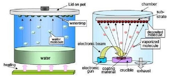
Vacuum deposited PVD coatings are used for decorative coatings, vapor barrier layers, metallic conductors and corrosion resistant coatings. Vacuum evaporation uses an evaporation source where material is thermally vaporized from a heated container, much like how water vapor is evaporated by boiling, as shown in Figure 3. The evaporation source, which can be heated electrically or by an electron beam (e-beam) thermally vaporizes the evaporant. The vaporization is done in a good vacuum so the trajectory of the vaporized a material is line-of-sight. The vacuum environment reduces contamination from the environment. Typically the gas pressure range is 10-5 to 10-6 Torr.
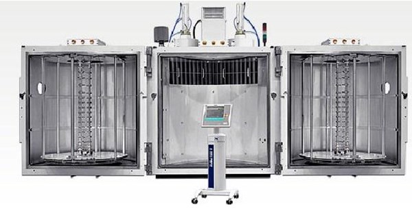
One advantage of vacuum evaporation is that the source material can be as simple as granulated solids at any desired purity. Figure 4 shows a production evaporation machine by Leybold Optics; it is built using 2 clamshell doors for rapid loading and unloading of parts. Because of the line-of-sight trajectory masking may be used to define the region of deposition in many cases.
One disadvantage of vacuum evaporation is in the deposition of alloys or compounds where it can be difficult to deposit coatings with proper composition or stoichiometry. Another disadvantage is that there may be a low utilization of source material. Very few process controls are available for tuning of coating properties. For complex surfaces proper fixturing is necessary to get uniform coatings so moving holders are used to gain uniformity. Depending on the melting point of the source material high heat loads in the chamber may be encountered.
Fig. 3. Vacuum evaporation deposition (right) showing a physical parallel with water evaporation and condensation (left). As an example of vacuum evaporation an e-beam is used to evaporate the source material (right). [image courtesy of NIDEK Int., Japan]
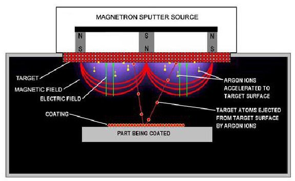
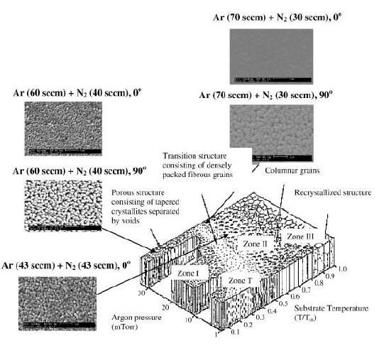
In sputtering, atoms are removed from the solid “target” by bombardment by accelerated ions. Momentum transfer causes the ejection of surface atoms, which are then deposited onto the substrate. Sputtering occurs at <5 x 10⁻³Torr where particles do not suffer from collisions with gas molecules in the space between the target and part. The various types of sputtering including diode, magnetron and ion beam sputtering as shown in Figure 2. A schematic of a magnetron sputtering process is shown in Figure 5. A confining electric and magnetic field cause electrons to circulate in the field over the target creating a plasma region. Ions are accelerated from the plasma to the target by an accelerating potential. The plasma glow generated is shown in Figure 6 for a lab size coater. With the advent of rotatable magnetron sources, target utilization has improved and has allowed very large areas to be economically coated, such as 3.3 m x 6 m “jumbo” flat glass. Figure 7 shows a Hauzer commercial sputter coater for bulk part coating. The advantages of sputtering are a wide range of metal, alloys and compounds can be sputter deposited. A range of coating microstructures can be obtained by variation of pressure and part temperature. Figure 8 shows how a range of corrosion resistant CrN microstructures that can be obtained following the Thornton diagram for sputter deposition. Sputter sources have been well developed and provide good target utilization. Reactive gases can be used to deposit compound materials.
One disadvantage of sputter deposition is that sputter deposition rates are lower than thermal evaporation rates and the film properties also depend on angle-of-incidence of the flux of particles. Generally the flux is non-uniform, but fixturing can reduce non-uniformity. Another consideration is that the sputtering targets are expensive relative to evaporant sources..
Fig. 5. Schematic of a d.c. magnetron sputtering process in a sputter down configuration. Not shown in the figure are the confined electrons within the electric field. [image source: Marca Coating Technology, LLC, Scarborough, ME, www.marcacoating.com],
Fig. 6. Photo of a lab size d.c. magnetron sputtering system in operation, showing the plasma discharge. [Image Source: GaLa Intrumente, GmbH, Bad Schwalbach, Germany]
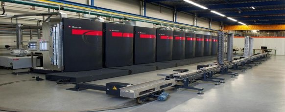
Fig. 7. A modular production sputtering/PECVD coating system. The coater uses a rack system 1.5 x 1.2 m x 0.2 m deep. Coatings for decorative, corrosion resistance and wear applications can be made on this system. [image courtesy of Hauzer, Veno, NL].
Fig. 8. The range of CrN microstructures achieved by sputtering as shown, corresponding to the Thornton Zone Diagram. CrN is used as a corrosion resistant coating. The Thornton diagram shows the relationship of microstructure with the effects of substrate temperature and argon pressure [image courtesy of Elsevier, Pulugurtha, 2007]
Sputtering by HIPIMS
A fairly new type of sputtering is known as high impulse power magnetron sputtering or HIPIMS. (also known as HiPPS and HPPS). HIPIMS uses very short pulses of high power to the target of the order of kW/cm2. This increases the ionization of the sputtered material creating a metal-based plasma. This contrasts with a gas plasma of normal sputtering. Since the duty cycle is small (<10%) the average heating of the target is manageable. Coatings made by HIPIMS are very dense and smooth in character. Much of this work is still in development, but pulse power supplies are available. Metals including Cu, Ta, Ti, and oxides such as TiO2, ZnO, InSnO, ZrO2 have been deposited using HIPIMS. Also, anti-corrosion coatings of TiN, CrN/NbN and CrAlYN/CrN and CNx hard coatings have been made by HIPIMS.
Ion Plating
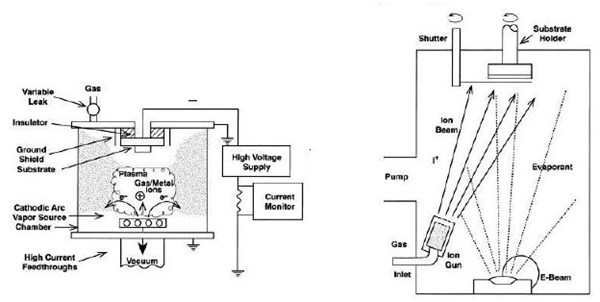
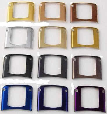
Ion plating uses energetic ion bombardment during deposition to densify the deposit and control properties of the coating such as stress and microstructure. Ion bombardment during deposition can be done by accelerating ions from a plasma to the part or by using a separate ion source (ion “gun”) as shown in Figure 2. Figure 9 shows an example of plasma-based ion plating (left) and ion beam enhanced deposition (IBED) (right). In the case of plasma-based ion plating an accelerating potential is applied to the part being coated. In the ion beam case the ions are accelerated away from the ion source and the part can be at ground potential. Ion plating can be applied on most metallic, glass, ceramic, and even plastic surfaces. Shown in Fig. 10 is a range of colors created as a finish for parts such as a cell phone bezel.
Ion plating is used industrially to make hard coatings for wear surfaces, conformal coatings, and high-density coatings. Typical coatings produced by ion plating are include metals (Ag, Al, Au,Cu,Cr, Ni,Ti, Pt ); metal nitrides (TiN, Cr2N, Si3N4, AlN, ZrN); oxides (SiO2, Al2O3),carbides and diamond-like coatings (DLC). Coating thicknesses are in the range of 1 to 10 mm (40 to 400 μ-in.) Ion plating of aluminum (called IVD in Mititary Specifications) has proven effective for replacing cadmium in aerospace applications and has been used in several military and commercial aircraft systems, missiles, and helicopters. Ion plated aluminum outperforms cadmium in actual service tests and acidic salt fog. The Al coating does not induce hydrogen embrittlement and helps relieve problems with dissimilar metals and galvanic corrosion. Large capacity ion plating coaters are available. Examples of companies building equipment for the IBAD process are Veeco (Plainview, NY) and Vergusen Technology (Van Etten, NY).
The advantages of ion plating (including IBAD) are high energies are available at the surface of the part for bonding, surface coverage is better than evaporation and sputtering. Controlled ion bombardment of the surface can increase adhesion, density and relieve stress. Chemical reactions can be improved by supplying energy and by plasma activation of species over the surface.
Disadvantages of ion plating are that there are more processing variables than some of the other PVD techniques, uniformity issues may be present, there may be excessive substrate heating and residual compressive stress may form in some cases.
Fig. 9. Schematics of two ion plating configurations, on the right ion gun based system is also known as IBED. On the left is a plasma based ion plating system [after Mattox, 2007]
Fig. 10. Example of color range of ion beam plated parts.[image courtesy of Shenzen Kin Vacuum Tech., Ltd., Shenzhen, Guangdong, China]
Low-pressure CVD and PECVD
Chemical vapor deposition (CVD) and plasma enhanced CVD are methods to deposit atoms and molecules by reaction, reduction or decomposition of a chemical vapor species over a surface. In general some CVD reactions can be performed in atmospheric pressure or APCVD. Such APCVD reactions are used to form SnO2 on hot glass using SnCl4 or monobutyltin trichloride and dopants to make Low-e coatings. Many CVD reaction byproducts contain hot volatile by products such as H2, Cl2, HCl, HF or water vapor. So venting, scrubbing of byproducts and unreacted species is required. Depending on the byproducts there are potentially more environmental issues compared to PVD. Another issue is the cost of the precursors, especially organometallics. Sub-atmospheric or Low pressure CVD is used to control reactions and too exclude ambient air and water vapor from the reaction. Traditionally CVD has been thermally driven processes requiring the substrate to be heated to fairly high temperatures (e.g. 300-600 C). Plasma enhancement can help decompose, activate or reduce the reactant so it can form the coating at lower temperatures. Typical coatings produced by CVD are metals such as nickel, tungsten, and titanium; carbides, such as TiC and W2C; oxides such as SiO2 and Si3N4; silicides such as WSi and TaSi; and semiconductors like silicon. Some of the coatings are very refractory in nature and difficult to make by other methods. Many of these processes are used in the semiconductor industry. A commercial size PECVD coater is shown in Figure 11.
Fig. 11. PE-CVD three station vertical glass coater, for a-silicon, metallization and sputter etching, 0.4 x 0.4 m processing area. [photo image courtesy of Von Ardenne, Dresden, Germany; Perrysburg, OH ]
Atomic Layer Deposition (ALD)
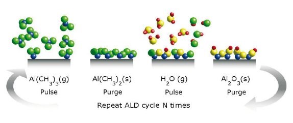
Atomic layer deposition (ALD) is a form of CVD where two or more chemical vapor precursors react sequentially over a surface, causing a self-limiting surface reaction and forming a thin molecular film a few angstroms thick. An inert carrier gas is used in which the reactants and carrier flows over the surface. Forming a traveling wave over the surface where the precursors are injected as pulses of chemicals. This is followed by pumping, purging the surface. This pulse purge process is shown in Figure 12. For Al2O3 deposition the system is maintained at 0.1-10 mBar over typical temperatures of 50-500 C depending on the reactants. The process is repeated in a sequential fashion to build up the coating. The process tends be slow but gives very complete surface coverage, making it ideal for barrier or interfacial coatings. This is a self-limiting reaction since when one the precursors are consumed the reaction stops. The speed to put down any coating of reasonable thickness is slow relative to other processes. The ALD coating is a conformal, pinhole free coating. The coating can uniformly cover even blind taps, up to a 70:1 aspect ratio. A couple companies offer commercial ALD coating machines. One example is shown in Figure 13. ALS is just beginning to be adopted for Al2O3, TiO2 and ZnS commercial coating. However, many types of materials including nano-laminates and doped materials have been made by ALD.
The materials include: metalssuch as: Ir, Pd, Pt, Ru; metal oxides: Al2O3, CaO, CuO, Er2O3, Ga2O3, HfO2, La2O3, MgO, Nb2O5, Sc2O3, SiO2, Ta2O5, TiO2, VXOY, Y2O3, Yb2O3, ZnO, ZrO. Metal. nitrides: AlN, GaN, TaNX, TiAlN, TiNX . Metal carbides and sulfides:TaC, TiC, ZnS, SrS. Fluorides: CaF2, LaF3, MgF2, SrF2and the polymers: PMDA–DAH, PMDA–ODA [Beneq, 2012].Since ALD creates such a conformal and very low defect coating it is ideal for oxygen and water vapor barrier coatings sought by the electronics industry and packaging industry. ALD is used to make seed layers as a base for subsequent processing. Copper seed layers have been used for Cu Electroplating and tungsten (W) seed layers have been used to assist in W metal deposition.
Fig.12. ALD process to deposit Al2O3 over a surface. This shows a 4 step cycle involving an aluminum precursor (trimethylaluminum) pulse, purge, water vapor pulse forming Al2O3 followed by a purge. An example growth rate is 0.8A/cycle at 300-450 C. [image provided by Beneq Oy, Vantaa,Finland]http://www.beneq.com/atomic-layer-deposition.html.
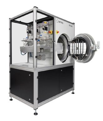
Fig.13. Batch production Atomic layer Deposition (ALD) showing 0.8 m x1.6 m chamber. Larger flexible roll based systems have also been made. [image provide by Beneq, Vantaa, Finland]
Product finishers who use PVD and Dual Processes
Several finishing companies use PVD to make coatings to replace electrodeposited finishes. Delta Faucet (Indianapolis, IN) was the first company to use PVD to create anti-tarnish decorative faucet finishes. Delta is so confident in these PVD coatings that they guarantee these finishes for life to never tarnish, corrode or discolor. Kohler (Sheboygan, WI) is another company who embraced PVD for decorative coating. Deco Plas (Montpelier, OH) uses PVD to deposit chromium and other finishes on a variety of plastics for automotive parts. The process involves cold plasma cleaning, which cleans the part on the molecular level and eliminates static electricity. Cleaning is followed by robotic painting, and UV curing, the parts are transferred to PVD chamber and coated with chromium (Nano-Cr-Chrome). This is done in 6’ wide x 6’ tall x 8’ deep chamber. The last process is a clear coat using UV cured polymer [Destefani, 2009]. At the Kalcor Company (Willoughby, OH) a mid-coat system has been developed, using a PVD coating as the second layer. This PVD coating is covered by two top layers giving greater range of color and depth.[Mills and Adams, 2009].
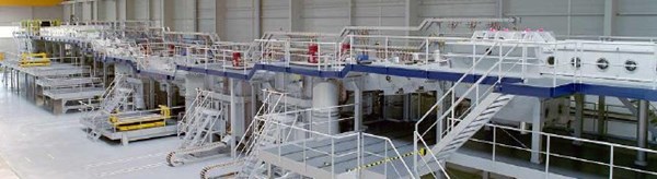
For many years black coatings were made by electroplating, including black chrome, black nickel, black gold, black rhodium. Some of these coating has been replaced by black diamond like carbon (DLC). In some cases black DLC is used for wear applications. Many of the DLC coatings are produced by reactive magnetron sputtering. DLC coatings of the type tetra -amorphous carbon are made by sputtering or cathodic arc. They can be very hard, but also brittle due to internal stress. The other type amorphous hydrogenated carbon (a-C:H ) are thicker, not as hard but resistant to corrosion. Other DLC coatings can contain some diamond microstructures. The solar field, which uses such coatings as black chrome and black nickel, graded metal-metal oxides can now use PVD coaters to coat metal strip for collectors. A large-area metal strip coater for coating solar absorbers is show in Figure 14.
Fig. 14. A large-scale production coater making coated solar absorber metal strip. This is used for making reflectors and absorbers for solar thermal collectors. The strip width is 1.250 m. The plant capacity is 6 million m2/yr. [Image courtesy of Von Ardenne, Dresden, Germany]
PVD Coating Facility
The typical vacuum deposition plant consists of several sections. The main coating chamber contains sources and fixturing for parts to be coated, a gas supply system (for back fill or reactants), a pumping system (containing roughing pumps and diffusion pumps), electrical supply system (D.C. and R.F are common), and control and monitoring systems. A schematic of a setup for ion plating using electron beam evaporation is shown in Figure 15.
Fig. 15. Equipment configuration showing the deposition chamber, pumping, gas and electrical feeds. This configuration shows an ion plating system with an e-beam evaporation source. [image courtesy of Elsevier, Chou, 2001].
Cleaning in PVD
Cleaning in PVD processing is divided into two stages. The first is cleaning external to the deposition chamber. This includes storage and handling prior to insertion into the deposition chamber. The second is the cleaning that can be done in the deposition chamber (i.e. in situ cleaning). External cleaning technologies are well established and will not be discussed further. In situ cleaning can be done in the deposition chamber by sputtering the surface of the part by ion bombardment with inert gas ions. This is an integral part of the ion plating process but can be used with other PVD processes as well.
Economic issues in coating processing selection
Consideration of the economic issues in the selection of a coating should include the total cost to produce a coated part, sourcing issues, the life of the coating and associated operating maintenance costs and additional benefits of the coating. All of these must be included when comparing coatings for a given application. The total cost to produce a coated part includes at least the following cost: substrate preparation, cleaning, coating cost including fixturing, masking, and deposition and consumables. Cost should include final sealing as necessary and subsequent finishing and quality control and yield. Costs incurred in quality control are usually more than compensated for in reduced rework. All of these cost components contain labor costs and amortization of equipment. Also, the cost of effluent control and waste disposal can be a big factor. Training cost for labor must be included. Running and trouble-shooting PVD systems requires specialized training unique from plating and other finishing operations.
When analyzing costs, the total life cycle must be considered. These include the life of the coating, whether or not the part can be recoated (replacement or refurbishment costs), and the cost of downtime when the coated part must be removed from service and replaced (lost production and labor and other costs). Each coating offers its own set of potential benefits that should be included in any economic analysis. A first consideration is whether or not a coating is an enabling technology. A specific coating may enable a whole new process or product replacing an existing one, or makes a substantial improvement on the existing one. Whether enabling or not, a coating frequently improves the quality of the product. In other applications, coatings can also improve safety, reduce liability risk, and reduce warranty costs.[Tucker, 2004].
The main barrier with PVD technology is high capital cost as new production systems typically cost a minimum of several hundred thousand dollars. PVD systems can operate at high temperatures and vacuums, requiring special operating considerations. Even with the relatively high capital cost and special operations requirements, PVD technology has shown the ability to replace conventional wet processes and provide superior coating performance for certain applications while eliminating environmental, health, and safety issues with wet processes using metals like chromium and cadmium.
Conclusion
As one can see there are many resources and experiences with PVD, PECVD, ALD as industrial coating processes. Many different vacuum deposited coatings are available for a variety of applications including decorative, wear, and corrosion resistance. Many of these processes are industrialized and equipment manufacturers have experience with making large scale production machinery. Some traditional electroplating companies have converted or use dual process to make quality coatings, while reducing environmental impacts. So as a finisher if you want to investigate is area deeper please see our Society of Vacuum Coaters web site at www.svc.org (505-856-7188) for a listing of educational courses, webinars, including on-site tailored courses, technical conferences, technical blog spot, and company contacts. The Society of Vacuum Coaters is a non-profit organization with membership open to all.
Dunn, G (2012) NASF (Nat. Assoc. for Surf. Fin.) “U.S. EPA Publishes Final Chromium Air Standards” http://www.nasf.org/nasf-law-regulation.php
Fed. Reg.(2012) v77. No 182, 19 Sept. 2012, National Emission Standards for Hazardous Air Pollutant Emissions:Hard and Decorative Chromium Electroplating and Chromium Anodizing Tanks; and Steel Pickling—HCl Process Facilities and Hydrochloric Acid Regeneration Plants
1309.
Mattox,D. (2007) “SVC Education guide to vacuum deposition technology”, available from. www.svc.org
Mattox, D. and Mattox, V.H., (2007) 50 years of vacuum coating technology and the growth of the Society of Vacuum Coaters, Soc. of Vac. Coaters, Albuquerque, NM, www.svc.org.
Mills,P. Adams,J. (2009), Beyond the Bling - PVD/UV Coating Systems that offer more than Beauty and Brawn, Plastics Decorating, July/August 2009
Pulugurtha,S.R.(2007), Bhat, D.G., Gordon, M.H., Schultz, J. “Effect of substrate orientation on film properties using AC reactive magnetron sputtering” Surf. And Coat. Tech. 202(2007), 755-761.
The author wishes to thank, Dr. Donald M. Mattox, MPI (formerly Sandia Labs), Mr. Ric Shimshock, MLD Technologies, Inc. and Prof. Ludvik Martinu, Univ. Montreal, for their review and comments. Also, the author wishes to thank the companies mentioned for use of their figures.
Author Bio: Dr. Carl M. Lampert is the Technical Director of the Society of Vacuum Coaters; Dr. Lampert is a consultant and managing partner of Star Science. He holds three degrees from University of California, Berkeley, CA in Materials Science and Electrical Engineering. His work has spanned many different types of coating processes and characterization. He has worked on the characterization and aging of electrodeposited solar absorbers, black chrome and black nickel in the late 1970’s. He has worked with both electroplated and sputtered coating of tungsten and nickel and molybdenum oxides. He headed a group at LBNL using sputtering, electrodeposition and sol-gel coating methods. He consults for companies on transparent conductors, flexible displays, active coatings for satellite thermal control, nanocrystalline coatings, smart windows, electrochromics, concentrating photovoltaics for space. He has been involved with CVD of TCOs on glass. He consults on business plans, writes and reviews proposals. Carl has been involved with start-up companies. One company, Life-Space-Art, makes inkjet deposited digital images on large glass sheets. Carl serves as the Technical Advisor on two corporate boards and is a, fellow of SPIE, and member of ACS, ASM, Et Kappa Nu, IEEE, Sigma Xi, and SVC.
Bryan Leiker, executive director for the Metal Finishers Association of California (MFACA), offers an update on actions to counter a proposed ban on hexavalent chromium plating and anodizing operations in the state.
Regulatory pressures to switch from hexavalent chromium to trivalent alternatives are a growing concern for many finishing operations. In this Products Finishing Ask the Expert clinic, Brittany McKinney of Pavco discusses the environmental considerations driving these regulations.
The advantages of boric acid-free nickel plating include allowing manufacturers who utilize nickel plating to keep up the ever-changing regulatory policies and support sustainability efforts.
While problems continue to rise with using lead anodes for hard chrome plating, some manufacturers are discovering platinized titanium anodes as a much-improved alternative with a long list of advantages.
Although Chevrolet has announced the end of the Camaro and Dodge is offering “Last Call” editions of the Charger and Challenger, the Ford Mustang is launching to its seventh generation.


.jpg;maxWidth=600)
.jpg;maxWidth=600)

.jpg;maxWidth=600)


