
AES Research Project #41: Plating on Anodized Aluminum; Part 3: Pore Structure and Bonding
The effect of anodizing voltage on the adhesion of nickel electrodeposited on anodized aluminum is related to the morphology of the anodic film. In general, adhesion is a linear function of the applied anodizing voltage. New data on the initial stages of pore formation during anodizing indicate that: (1) that the growth mechanism during the initial stage (< 10 sec) differs from that during subsequent growth, (2) there is no metallic bonding and (3) electrodeposited nickel coatings typically fill the entire pore.
Share


by
D. S. Lashmore


Editor's Note: Originally published as D.S. Lashmore, Plating and Surface Finishing, 68 (4), 48-51 (1981), this paper was the third of several reports on AES Research Project #41, a study of the technology of plating on aluminum, at the National Bureau of Standards, now the National Institute for Science and Technology. A printable version of this paper can be accessed HERE.
ABSTRACT
The effect of anodizing voltage on the adhesion of nickel electrodeposited on anodized aluminum is related to the morphology of the anodic film. In general, adhesion is a linear function of the applied anodizing voltage. New data on the initial stages of pore formation during anodizing indicate: (1) that the growth mechanism during the initial stage (< 10 sec) differs from that during subsequent growth, (2) that there is no metallic bonding and (3) that electrodeposited nickel coatings typically fill the entire pore.
Introduction
Anodizing has been used as a pretreatment for plating on aluminum for almost 50 years, as was recently reviewed.1 In spite of a long history, anodic pretreatments are not as common as the zincate and stannate processes. Apparently, the reason for this lack of popularity lies both in low adhesion on certain alloys and in the large power requirement of existing processes. Inherent in the anodizing process, however, are a number of advantages, including the low cost of chemicals, freedom from electrolytes that contain cyanide, and low waste-treatment costs.
The anodizing processes take advantage of the oxidation characteristics of aluminum, and, in particular, the ability to form a porous anodic film under certain electrochemical conditions. Immersion processes require a complete removal of the aluminum oxide (in an aqueous electrolyte) and some dissolution of the substrate in order to deposit a continuous metal film. In addition, cyanide-containing solutions are often involved.
The microstructure of porous anodic films formed in common electrolytes such as dilute phosphoric, sulfuric or oxalic acid on pure (~99%) aluminum has been investigated extensively.2-10 However, the nature of nickel deposits on porous anodic films has not been studied.
In this paper the work of previous investigators concerning the initial stages of anodic film formation and film structure is extended to include the morphology of anodic films on 7000-series alloys and the morphology of nickel coatings plated on these porous films. The first transmission electron micrographs of cross sections of nickel coatings on anodic films are presented along with adhesion measurements which, together, relate the structure to adhesion.
Adhesion vs. anodizing voltage
The adhesion of nickel plated on porous anodic films formed on aluminum alloy (7146-T63) was measured by peel testing.11 The specimens, typically 5 × 10 × 0.64 cm, were buffed and degreased with trichloroethylene in an ultrasonic cleaner. The specimens were then polished with 0.01 μm MgO, given a 30-sec ultrasonic cleaning in 50% aqueous nitric acid, rinsed in distilled water and immediately anodized according to the procedure described by Wittrock12-14 (Table 1). The total charge density was standardized at about 20 coulombs/cm2 regardless of the anodizing time.
After anodizing, the specimens were immersed in an electrolyte containing 2 g/L sulfamic acid maintained at 55-60°C, rinsed in distilled water, and transferred to a nickel sulfamate electrolyte maintained at pH 2.5. The specimens were held in this solution for 60 sec prior to applying a voltage. The voltage was applied at a slow rate so that the current density increased from 0 to 4.3 A/dm2 in about 5 min. All specimens were plated with 150 μm of nickel.
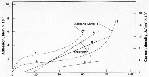
Figure 1 - Adhesion and current density as a function of anodizing voltage: (A) 10% H3P04, 60°C; (B) 3% H3P04, 60°C; (C) 10% H3P04, 30°C.
As shown in Fig. 1, the adhesion was found to be approximately a linear function of anodizing voltage, neglecting the data for the first 10 to 15 volts. The slope of the curve changed with the concentration of phosphoric acid. The current density versus the applied voltage has been superimposed on Fig. 1, revealing that the greatest adhesion occurs when the current density rises abruptly. It should be noted that the limiting current density depends on the degree of agitation, which in this case was produced by a mechanical stirring rod. Therefore, the current-density curves may not be quite accurate, even though mixing was vigorous.
The electrodeposited nickel coatings are in contact with a very large surface area of the anodic film. The contact area is made up of both the total area of the pore walls, the bottom of the pores and the remaining outer surface of the oxide. Generally, the wall area of the pores is the largest contributor to the contact area and is plotted as a function of applied voltage in Fig. 2. This curve was calculated from the data of O'Sullivan and Wood3 and assumes that the pore diameter is a linear function of voltage and that the pore population, N, is proportional to the inverse of the voltage squared. If adhesion between nickel and the substrate was dependent upon the contact area between the nickel and the aluminum oxide, then the adhesion would be expected to decrease as the voltage increased (with an increase in surface area). However, Fig. 1 clearly shows that adhesion increases as the voltage increases. Keller, Hunter and Robinson2 showed that the structure of the anodic film is not a very sensitive function of the nature of the electrolyte for phosphoric, chromic and oxalic acids (at a given voltage). This is especially true at higher voltages where the pore densities (surface area available for bonding) are within about 30 percent of each other in the anodic coatings obtained in all three acids. The adhesion, however, is highly dependent on the nature of the electrolyte and also upon the type of aluminum alloy. Because the most obvious difference is in the composition of the anodic film itself, one may deduce that the composition of the anodic film governs the adhesion of subsequent nickel (copper or other) coatings and that, most probably, the composition is changed with graduation of the applied voltage.
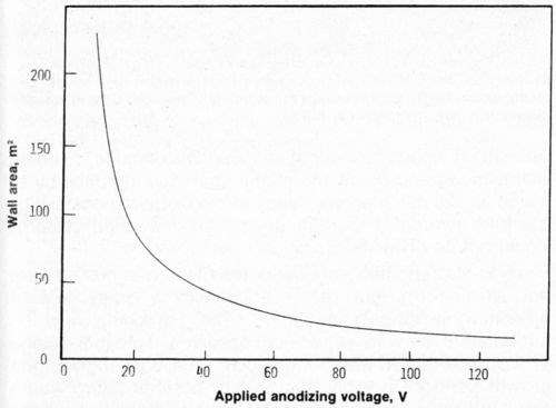
Figure 2 - Bonding surface area (wall area) as a function of applied voltage.
Post-anodizing treatments can improve adhesion. Wittrock found that treatment in a sulfamic acid solution yields larger peel-test values for subsequently deposited nickel layers. Preliminary results during this program indicate that HF (0.5 vol%) is even more effective. However, if the concentration of HF is increased to 2 g/L, then the adhesion will drop off. Strong solutions of HF obviously attack the oxide, whereas sulfamic acid solutions do not to any appreciable extent. A possible explanation for the effect of the post-anodizing treatment is that a weak boundary layer is removed from the pore walls and, most probably, reaction products are removed as well.
Microstructure of anodic films
In order to better understand the above observations about adhesion, the microstructure of anodic films was investigated using transmission electron microscopy (TEM). Two different alloys (7129-T63 and 7146-T6) were investigated. Specimens were prepared in two ways, so that the interface was either perpendicular or parallel to the electron beam. No previous data for the latter have been reported in the literature; therefore, this investigation represents the first direct TEM study of nickel plated on an anodic film.
Foils suitable for TEM were prepared by anodizing in accordance with Wittrock's procedure12-14 and then plating with nickel from a sulfamate electrolyte for a short time as described above. After measuring the adhesion, nickel was again plated on the specimen to a thickness of about 1 cm. Sections were prepared from these specimens in such a way that the plane of the cut was perpendicular to the plane of the interface. Two methods - spark cutting and sawing with a low-speed diamond cut-off wheel - were used to sever the specimens. The thickness of the sections varied from 75 to 250 μm. Sections prepared by spark cutting were further polished using standard metallographic techniques and 0.01-μm MgO in the final step. The specimens prepared with the diamond cut-off saw were used without further processing. Both sets of sections were thinned to electron transparency in an ion milling machine with milling times in excess of 7 days, operating 24 hr/day. The thinned foils were examined at 100 keV in a transmission electron microscope equipped with an anti-contamination stage and a double-tilt specimen holder.
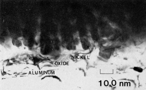
Figure 3 - Transmission electron micrograph of nickel electrodeposited on 7129-T6 alloy anodized in 4% phosphoric acid (100 keV, B.F.).
A representative micrograph of 7129-T63 anodized in 3.0% phosphoric acid is shown in Fig. 3. The adhesion measured by the peel test exceeded 75 N/m (100 lb/in.). The average cell size at the interface was about 125 nm, yielding a cell density of 6.4 x 10⁹ cells/cm, which is in approximate agreement with the data of Keller, Hunter and Robinson.2 The pore (end) radius was about 0.85 nm. Several important structural features of the anodic oxide nickel system are revealed in Fig. 3. First, the nickel filled the pores completely. Secondly, there appears to be a continuous oxide barrier between the nickel and the aluminum substrate. The substrate in this case was not oriented for dislocation contrast, so the effect of the aluminum structure on the growth of the anodic film was not apparent. The structure, however, has a very important effect on the growth of the film, especially during the initial stages of growth. It is seen in Fig. 4, for example, that in several places the oxide appears to have penetrated along the dislocations. Regions of oxide, 15 nm in diameter, extend below the aluminum/oxide interface by as much as 120 nm. Moreover, many of the oxide regions exhibit fourfold symmetry, though crystalline diffraction patterns could not be observed.
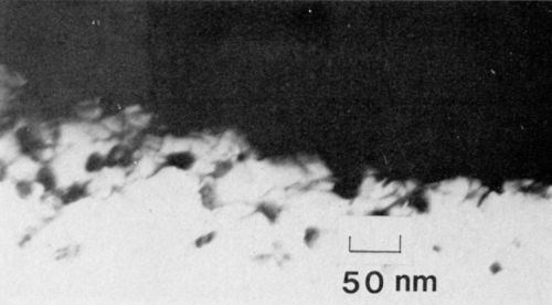
Figure 4 - Transmission electron micrograph of nickel-plated anodized 7129-T63 alloy showing oxide growth along dislocation near the interface (100 keV, B.F.).
It was also apparent that the pores (filled with nickel) were not all uniform, but rather underwent a great deal of branching as shown in Fig. 5. The branching may be attributed to the voltage transient observed at the initial stage of film growth and which may occur locally throughout the growth period. Certainly, this type of pore structure would result in a strong mechanical bond between the nickel and the oxide.
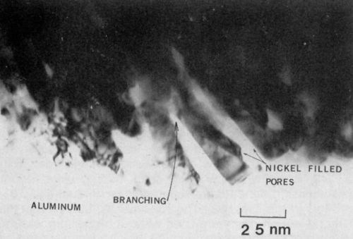
Figure 5 - Transmission electron micrograph of nickel-plated anodized aluminum showing pore branching in the vicinity of the interface (100 keV, B.F.).
The initial stages of growth of the anodic film on specimens of 7146-T6 alloy were studied by TEM with the beam perpendicular to the interface. These specimens were prepared by thinning to electron transparency and anodizing for various periods of time. Figure 6 is a micrograph of a specimen anodized for 10 sec and indicates that the mechanism of the initial film formation is apparently different from that of growth during a latter stage. A large number of rectangular and square regions of oxide were observed on the (100) plane of the 7146-T6 alloy. This indicates that a role is played by the crystal structure of the substrate. These regions of oxide grow in such a way as to form pores, as indicated in the micrograph. Even the large pores show evidence of being made of rectangular "building blocks" of oxide. An additional feature observed in the initial stage of film formation is a large number of fringe areas that may be Moiré fringes.
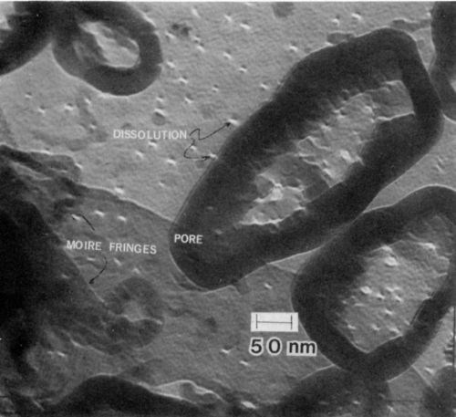
Figure 6 - Transmission electron micrograph of the initial stage of growth of anodic film on 7146-T6 alloy. Note the many square regions of oxide on (100)-oriented substrate (100 keV, B.F.).
In the initial stages of film formation, field-assisted dissolution at the base of the pores does not occur. The white areas in Fig. 6 are etch pits that are remote from the pores. Some pores contain dissolution sites, but many do not. Thus, the film formation mechanism that occurs initially can be quite different from that occurring at later times. Further evidence supporting this observation is shown in Fig. 7, where aluminum dissolution was observed to occur outside of a large pore. In Fig. 7, a number of well-developed pores are also observed to have no evidence of dissolution at their base. The base of some pores seems to have been filled with oxide. It is thought, however, that once the surface is uniformly covered the oxide will dissolve within the base of the pore by the well-established field dissolution mechanism. Very large regions of oxide with fourfold symmetry are apparent in the micrograph.
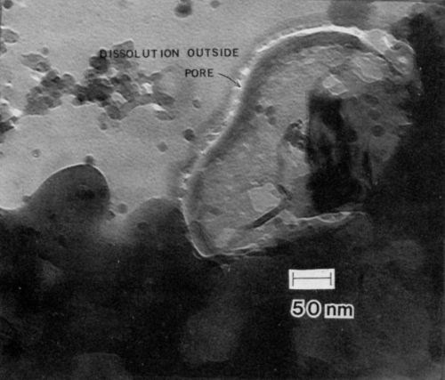
Figure 7 - Transmission electron micrograph of the initial stage of formation anodic film on 7146-T6 alloy, showing dissolution on the outside of the re (100 keV, B.F.).
At a later stage of growth, the pores have a more classical appearance as shown in Fig. 8, a specimen anodized for 30 sec. In this micrograph the interface is perpendicular to the electron beam. The transition from small to larger pores is clearly seen in this dark-field micrograph taken with the electrons scattered by the amorphous oxide.
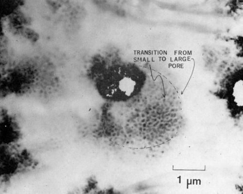
Figure 8 - Transmission electron micrograph of a later stage of formation of anodic film on 7129-T63 alloy, showing the transition of a small pore diameter to a larger pore diameter (branching). The beam is parallel to the direction of growth (100 keV, B.F.).
Conclusions
Data reported in this paper show that:
- The adhesion of nickel to anodized aluminum is approximately a linear function of the applied voltage during anodizing.
- The adhesion must be a function of the composition of the film itself and that this composition is affected by the applied voltage.
- Transmission electron micrographs of cross sections of nickel plated on a porous anodic film reveal that nickel completely fills the pores, and that there is no evidence of metallic bonding (i.e., no metal-to-metal contact).
Acknowledgments
The author thanks the Aluminum Association and the American Electroplaters' Society for the financial support of AES Research Project 41, under which this work was conducted. The author also thanks Dr. Ugo Bertocci and Dr. Ellio Passaglia for their comments on the manuscript.
References
1. D.S. Lashmore, Met. Fin., 78, 21 (1980).
2. F. Keller, M.S. Hunter and D.L. Robinson, J. Electrochem. Soc., 100, 411 (1953).
3. J.P. O'Sullivan and G.C. Wood, Proc. Roy. Soc. London A, 317, 511 (1970).
4. G.E. Thompson, R.C. Ferneaux and G.C. Wood, Trans. Inst Met. Fin., 55, 117 (1977).
5. G.E. Thompson, R.C. Furneaux and G.C. Wood, Corr. Sci., 18, 481 (1978).
6. R.C. Ferneaux, G.E. Thompson and G.C. Wood, Corr. Sci., 18, 853 (1978).
7. G.E. Thompson, R.C. Ferneaux, G.C. Wood, J.A. Richardson and J.S. Goode, Nature, 272, 272 (1978).
8. G.E. Thompson, R.C. Ferneaux, G.C. Wood and R. Hutchings, J. Electrochem. Soc., 125, 1480 (1978).
9. G. E. Thompson, R. C. Ferneaux, J. S. Goode and G. C. Wood, Trans. Inst. Met. Fin., 56, 159 (1978).
10. G.E. Thompson, R.C. Ferneaux and G.C. Wood, Trans. Inst. Met. Fin., 57, 123 (1979).
11. H.J. Wittrock and L. Swanson, Plating, 49, 880 (1962).
12. H.J. Wittrock, Plating and Surface Finishing, 67, 44 (1980).
13. H.J. Wittrock, Proc. Am. Electroplaters’ Soc., 48, 52 (1961).
14. H.J. Wittrock, The Finishing of Aluminum, (G.H. Kissin, Ed.), Reinhold Publishing, New York, 1963; p. 163.
About the author (at time of publication)

Dr. David S. Lashmore is employed by the Chemical Stability and Corrosion Division, Corrosion and Electrodeposition Group of the National Bureau of Standards, U.S. Dept. of Commerce, Washington, DC. He received his Ph.D. degree in materials science from the University of Virginia, his M.S. degree in physics from Michigan Technological University, and his B.S. degree in engineering science and mechanics from the University of Florida. He has worked as a physics instructor and in other capacities and has authored several technical articles. Dr. Lashmore is a member of AES and Sigma Xi.


Related Content

Product Finishing’s 2024 Top Shops Benchmarking Survey Deadline Approaches
Taking this year’s Products Finishing’s annual Top Shops Benchmarking Survey? Respondents are urged to complete the survey by April 30, 2024 in order to be considered as a qualifying top shop.
Read More
Plasma Electrolytic Oxidation (PEO): A High-Performance Coating for Light Metal Alloys
Plasma Electrolytic Oxidation (PEO) offers an innovative approach to high-performance coatings for light metal alloys, providing superior alternatives to traditional hard anodizing. The process transforms the surface of metals like Al, Mg and Ti into a robust oxide layer with customizable properties, tailored for demanding applications in aerospace, semiconductor, and industrial manufacturing.
Read More
Products Finishing Reveals 2024 Qualifying Top Shops
PF reveals the qualifying shops in its annual Top Shops Benchmarking Survey — a program designed to offer shops insights into their overall performance in the industry.
Read More
Top Shop Aces Outstanding Customer Service
More than a finishing shop, this anodizing, powder coating and vacuum resin impregnating business goes above and beyond for its customers by being a resource for whatever their finishing needs might demand.
Read MoreRead Next

The Best Tape for High-Temperature Applications
High-temperature tapes are designed with maximum heat ratings indicating the highest temperature they can withstand for a very short time.
Read More
Reducing Material Use and Overspray
Looking for applicators or process improvements for reducing material use and overspray? Binks offers helpful advice for searching out new solutions.
Read More