
XRF Instrument for Micro-Feature Analysis
Bowman’s A Series Micro XRF quickly measures the smallest features on semiconductors and microelectronics.
#measurement-testing

Share
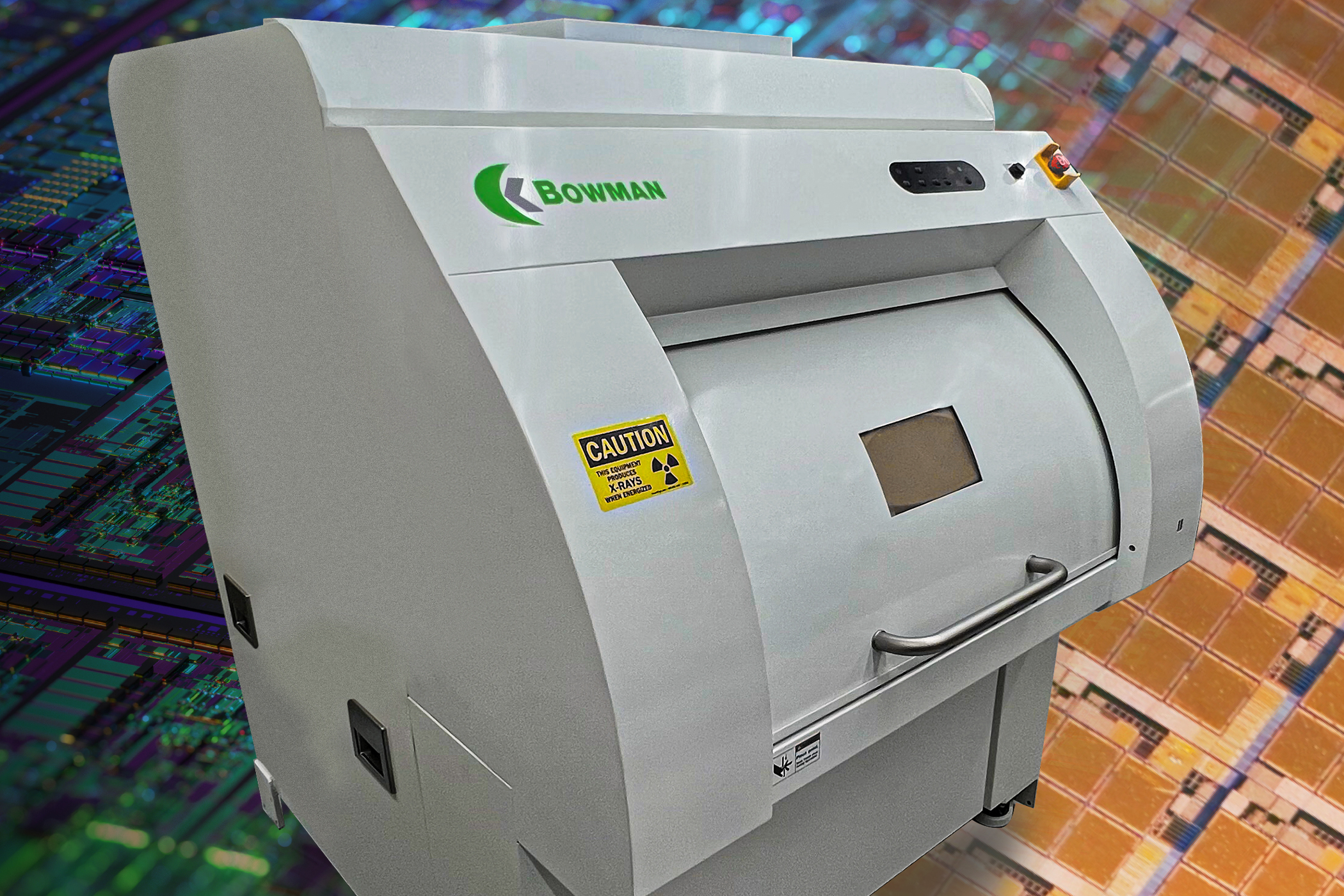
Bowman (Schaumburg, Illinois) has introduced a new addition to its suite of precision X-ray fluorescence (XRF) instruments used in the printed circuit board (PCB), semiconductor and microelectronics industries.
The Bowman A Series Micro XRF quickly measures the smallest features on semiconductors and microelectronics. It it said to accommodate very large PCB panels and wafers of any size for full sample coverage and multi-point programmable automation.
Poly-capillary optics focus the X-ray beam to 7.5 µm FWHM (full width at half maximum), which is reportedly the world’s smallest for XRF coating thickness analysis. A 140-times magnification camera measures features on that scale; a secondary, low magnification camera provides live-viewing of samples and “birds-eye” macro-view imaging. Bowman’s proprietary dual-camera system lets operators see the entire part, click the image to zoom with the high-mag camera and quickly identify the feature of interest.
A programmable X-Y stage with movement of 23.6" (600 mm) in each direction can handle the largest samples in the industry. The stage has precision down to ±1 µm for each axis, and is used to select and measure multiple points; Bowman pattern recognition software and auto-focus features also do this automatically. The system’s 3D mapping capability can be used to view the topography of electroless nickel immersion gold (ENIG), electroless nickel electroless palladium immersion gold (ENEPIG), electroless palladium immersion gold (EPIG) and other processes.
A Series instruments include 7.5 µm optics with molybdenum anode tube (chromium and tungsten also available) and a high-resolution, large-window silicon drift detector (SDD) which processes more than 2 million counts per second. SDDs are said to be the industry standard for complex thin films. The high count rate capability is key to achieving a low minimum detection limit (MDL) and highest spectral resolution.
According to Bowman, A Series systems are distinctive in that they are cleanroom ready, have the largest semiconductor stage movement on the market and are supported worldwide by a service network that provides same-day response for every benchtop XRF requirement. Equipment evaluation, selection, commissioning, maintenance and modernization is available for users of Bowman instruments, as well as other major XRF brands.
RELATED CONTENT
-
XRF Measurement System Fills Need for Multiuse Flexibility, Precision
The K Series is the ninth XRF in Bowman’s benchtop portfolio.
-
Bowman Showcases XRF Plating Thickness Measurement Systems
Photo Credit: Bowman Bowman says its X-ray fluorescence (XRF) plating thickness measurement systems are fast, accurate and also perform alloy analysis and solutions analysis.
-
Updated ED-XRF Analysis
The latest spectrometers from Spectro Analytical Instruments feature upgrades including improved spectra handling for increased screening method accuracy.


