ClassOne Provides Electroplating Solution for Diode Lasers
Appears in Print as: 'Solstice LT Benefits Superconductor Production'
ClassOne will provide its Solstice LT electroplating system to Jenoptik’s Berlin-Aldershof facility, where Jenoptik will produce semiconductors for high-power diode lasers.

Edited by Evan Doran
Share
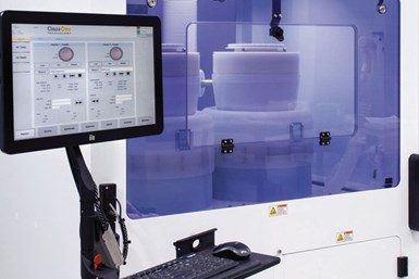
ClassOne Technology (Kalispell, Mont.) sold a Solstice LT electroplating system to Jenoptik (Jena, Germany) for manufacturing semiconductor material for high-power diode lasers at Jenoptik’s semiconductor production facility in Berlin-Adlershof, Germany. The dual-chambered Solstice LT is specially configured for high-performance gold processing. ClassOne says its GoldPro processing chamber offers exceptional levels of wafer-to-wafer, die-to-die, within-die and within-feature repeatability, improving product quality and reducing operating expenses.
The Solstice LT will allow Jenoptik to process different GaAs wafer sizes to accommodate different customer requirements, while also handling multiple wafer sizes on the same tool.
Jenoptik plans to use the Solstice LT to replace a manual plating wet bench. Dr. Juergen Sebastian, plant manager of Jenoptik’s Berlin-Adlershof facility, said the Solstice LT would “significantly improve process stability and plating quality as well as reduce our metallization step costs." Sebastian also praised the Solstice LT’s electrolyte technology, which he said promoted Jenoptik’s sustainability policy.
ClassOne Solstice systems provide high-performance electroplating specifically for ≤200mm wafer processing. The Solstice series includes fully-automated 8-chamber and 4-chamber systems with up to 75-wph throughput as well as a 2-chamber semiautomated configuration with process development and production functionality. In addition to electroplating, the Solstice platform’s unique Plating-Plus capabilities enable it to handle wafer cleaning, high-pressure metal lift-off, resist strip, UBM etch and other tasks.
RELATED CONTENT
-
Conveyors and Paint Systems
Choosing the right conveyor system, coating technology, and ancillary equipment.
-
A Protective Decorative Electrolytic Coloring Process for Aluminum
The main task of this work was to study the influence of the different parameters on the electrolytic coloring process for aluminum.
-
Troubleshooting for Electrocoating
Characterizing the type of defect is essential in identifying the root cause and eliminating its source...