The History of Electroplating and A Historical Review of the Evolution of NASF
The history of electroplating is a curious mixture of mistakes, observations, serendipity and experimental development, enmeshed and entwined with the discovery of electricity in the late 18th century. Join Mr. Nebiolo as he reviews the fascinating history of our industry and its metamorphosis during the last 238 years. He will also provide a brief history of our flagship society, the NASF.
#nasf #surfin
Share
by
William P. Nebiolo*
REM Surface Engineering
Southington, CT, USA
Editor’s Note: What follows is an edited manuscript based on a presentation given at NASF SUR/FIN 2022 in Rosemont, Illinois on June 7, 2022, in Conference Session 2: Metal Finishing: Past Present and Future. A printable PDF version of this report is available by clicking HERE.
Featured Content


ABSTRACT
The history of electroplating is a curious mixture of mistakes, observations, serendipity and experimental development, enmeshed and entwined with the discovery of electricity in the late 18th century. Join Mr. Nebiolo as he reviews the fascinating history of our industry and its metamorphosis during the last 238 years. He will also provide a brief history of our flagship society, the NASF. Have you ever wondered who was the first individual to electroplate something? Have you ever heard the term Galvanic action and pondered its origin? Are you aware that the French Emperor Napoleon played a role in our industry? Who discovered the first nickel brightener? These are just a few of the fascinating tidbits that will be shared in this fascinating, light-hearted and enjoyable presentation.
The History of Electroplating
Luigi Galvani (Fig. 1) was born in Bologna, Italy on September 9, 1737.1 As a young man, Galvani was interested in the field of theology. Encouraged by his parents to study the sciences, however, he instead enrolled at the University of Bologna in 1755 and received his Baccalaureate in Science in 1759.
Following his father’s preference for medicine, he then pursued as a graduate student the field of physiology and was awarded a medical degree in 1762. In 1781, the new and exciting science of the time was the recent discovery and study of electricity. In 1774, Galvani read a paper published by three authors; Leopoldo Caldani, Felice Fontana and Tommaso Laghi, who found that muscles in frogs, could be activated by the application of electrical stimulation. Curious of the claims in this paper, Galvani began his own series of experiments on severed frog legs, seeking to duplicate the findings of his peers and understand the phenomenon.

Figure 1 - Luigi Galvani: (a) Piazza Galvani, Bologna, Italy, circa 2017; (b) Italian physician Luigi Galvani.
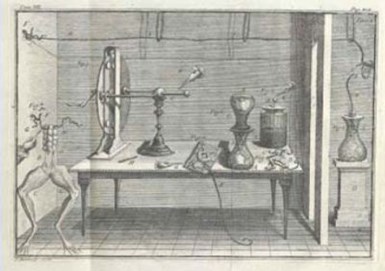
Figure 2 - A 1781 Drawing from Galvani’s notebook.
The image shown in Fig. 2, from Galvani’s laboratory notebook, shows that from 1774 to 1781, he used a hand-cranked static electricity generator and Leyden jar in his experiments. Touching the sciatic nerve in a severed frog’s leg; with a scalpel that had picked-up a charge from the Leyden jar, Galvani noted that the frog’s legs would indeed contract.1
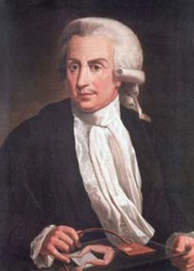
Figure 3 - Galvani with his frog and copper probe.
Continuing his experiments, Galvani made an interesting discovery. After pinning a frog’s leg to his lab table with a wrought iron nail; and before he connected the copper probe to the Leyden jar, he accidentally touched the frog’s sciatic nerve. To his surprise, the frog’s leg contracted. Galvani, however, was perplexed. How could this be since he hadn’t yet electrified his copper probe? He repeated the procedure with the same result and eventually concluded erroneously that the frog itself was its own source of electricity.1-4
Galvani had discovered what he called “animal electricity.”4 He claimed that an electrical fluid within the frog’s body was carried to the muscles by its nerves. After additional experimentation, Galvani determined that by connecting any two different metal probes in series with wires inserted into a frog’s leg, he could stimulate the leg to contract (Fig. 3).1,4
Alessandro Volta
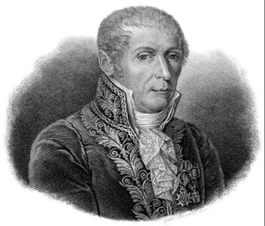
Figure 4 - Italian physicist Alessandro Volta.
In 1791, Galvani published the results of his experimentation and erroneous conclusion that the frog itself was the source of its own electricity. At the University in Padua, Italy, Italian physicist; Alessandro Volta (Fig. 4), read Galvani’s paper and began to expand upon Galvani’s animal electricity work. Volta eventually replaced the frog’s leg with a brine-soaked piece of paper. In doing so, Volta was able to detect the same flow of electricity that Galvani had detected, as long as the two probes that he used to connect to the brine-soaked paper in series, were made from dissimilar metals.1-4
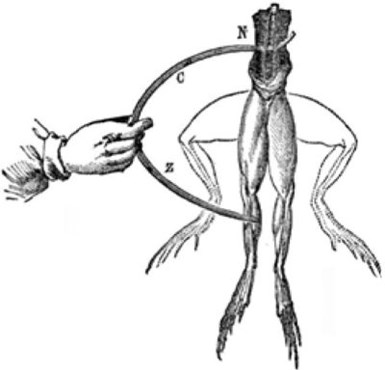
Figure 5 - Galvani notebook image of contracting leg.
Volta also determined that if the two probes were of identical metal, then there would be no flow of electricity. Volta had actually developed the first wet cell battery or as it was known at the time, a Voltaic Pile.3
It was Volta who realized that the frog’s leg in Galvani’s experiments; served as both the electrolyte; or carrier of the electrical current, and as the detector of the current, when the leg contracted (Fig. 5).

Figure 6 - Volta and his brine-soaked Voltaic Pile, circa 1799.
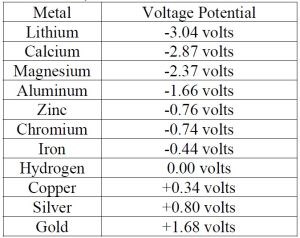
Table 1 – The Electromotive Series.1
The Voltaic Pile generates electrical current due to the difference in electrochemical potential between two different elements. This phenomenon is known as EMF, or electromotive force. The further the separation between two different elements, the larger the electromotive force that pair can generate when connected in series.2,3 By experimenting with different metals, Volta was able to generate a chart of the possible voltage potentials when anodes and cathodes of different metals are combined in a voltaic pile or a battery (Table 1).
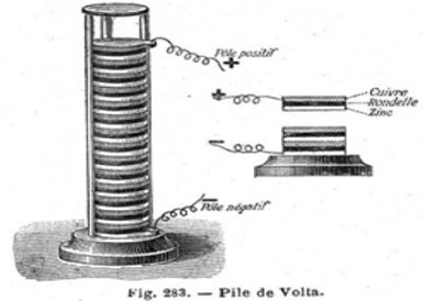
Figure 7 - The Voltaic pile of 1800. This first dependable, continuous source of D.C. electrical current.1
Volta’s first, practical, voltaic pile consisted of alternating layers of zinc and copper separated by brine-soaked cardboard to which a small amount of dilute sulfuric acid was added (Fig. 7).1-4 As a member of The French Institute of Science; the most prestigious scientific society of its day, Alessandra Volta travelled to France in 1801, where he demonstrated the Voltaic Pile before scientific colleagues and members of the Institute at the court of French Emperor Napoleon Bonaparte (Fig. 8).1,4
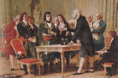
Figure 8 - Volta demonstrates the Voltaic Pile in 1801 at the court of Emperor Napoleon Bonaparte and French Institute of Science colleagues.
Volta’s Law or the Law of Electromotive Force states that the amount of electricity a battery will generate is proportional to the difference between the electrochemical potentials of the two metals used as its electrodes. To this day, electrical voltage is named in Volta’s honor for his discoveries and contributions. Likewise, the principle of Galvanic Action, wherein oxidation occurs at the anode and reduction occurs at the cathode, is named to honor Luigi Galvani.1
Luigi Brunatelli, the First Electroplater
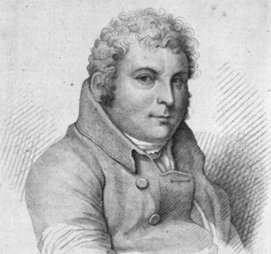
Figure 9 - Italian chemist Luigi Brugnatelli; 1805.1
A colleague of Alessandro Volta, also a member of the French Institute of Science, Italian chemist, Luigi Brugnatelli (Fig. 9), traveled to Paris in 1801, where he witnessed Volta’s demonstration of the voltaic pile.4 Intrigued with the device and proposing chemical experiments to be carried out with electricity, Brugnatelli was chartered under the auspices of the French Institute of Science and funded by the French government of Emperor Napoleon Bonaparte. He experimented with the voltaic pile at his chemical laboratory, upon returning to Italy. Four years later in 1805, Luigi Brugnatelli became the first person to electroplate another item.
Brugnatelli electroplated gold onto two silver medallions, by connecting them in series to a gold anode.4,5 All of the items were immersed in a brine solution and connected to a voltaic pile. The work, done under the auspices of the French Academy of Science, was ordered by Emperor Napoleon Bonaparte to remain a secret. This proclamation prohibited Brugnatelli from publishing of his scientific breakthrough, essentially, the development of electroplating. Thus suppressed, his work remained unknown for several decades until, he was allowed to publish a treatise on his electroplating developments in The Belgian Journal of Physics and Chemistry.5
The Contributions of Michael Faraday
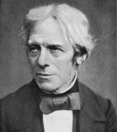
Figure 10 - Michael Faraday 1791-1867.1
The suppression of Brugnatelli’s developments prevented the discovery from being known in the scientific literature and as a result, the science of electroplating was reinvented in England. To that end, investigatory work on electricity continued in London, during the 1820s and 1830s at the laboratory of famed English scientist; Sir Humphry Davy.5 A protégé in Davy’s laboratory was chemist Michael Faraday (Fig. 10).6
In 1833, Faraday made some interesting observations during some of his experiments.3,4,5,7 Those observations led to the establishment of the laws of modern electroplating. To this day the laws still bear his name and establish electroplating operations on firm scientific principles.6 They are the basis for every electrolytic electroplating operation in use to this very day. Simply stated, Faraday’s First Law says that if you apply more current to the bath, you’ll deposit more metal.1
Faraday’s First Law of Electrodeposition
The amount of chemical change produced by an electric current; (i.e. the amount of metal deposited cathodically or dissolved anodically,) is proportional to the quantity of electricity passed through the plating bath.2,3,6
Faraday’s Second Law of Electrodeposition
The weight of different metals deposited or dissolved by the same quantity of electricity is proportional to their chemical equivalent weights.2,3,6
Simply stated, Faraday’s second law says, if the current remains the same, different metals deposit to different depths during the same period of time, dependent on their equivalent weight or valency.1 So for the non-chemists among us the question is, “What is a metal’s equivalent weight?”
The equivalent weight of a metal is simply its atomic weight, as found on the periodic chart, divided by its valence.6 For example, nickel has the atomic weight of 58.70 grams and a normal valence of 2. Therefore, its equivalent weight is 58.70 grams divided by 2, or 29.35 grams. Silver has an atomic weight of 108.87 grams and a valence of one, therefore, it has an equivalent weight of 108.87 grams divided by one, or 108.87 grams. By combining Faraday’s First and Second Laws, we are able to create the Metal Deposition Formula.3,6
Metal Deposition Formula
M = (I)(t)(E)(1/F) where:
M = Metal weight in grams deposited
I = current in amps
t = time in hours
E = the metal’s equivalent weight
1/F = amp-hour equivalent
But what is 1/F the amp hour equivalent? Faraday noted that a current of 1 amp for 1-second deposits 0.001118 grams of silver. Silver has an equivalent weight of 107.87 grams. By dividing silver’s equivalent weight of 107.78 grams by 0.001118 g of silver per second, Faraday determined that to deposit 107.78 grams of silver would require 96,494 amp-seconds.2,3,6 This has since been rounded up to 96,500 amp-seconds for convenience. In electroplating, amp-seconds are referred to as coulombs and the standard of 96,500 coulombs is called 1 Faraday, in honor of the scientist.6
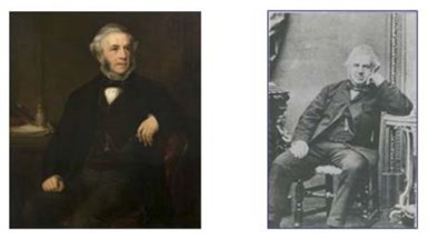
Brothers George and Henry Elkington.1
John Wright & the Elkingtons
Thirty-five years after Italian chemist Luigi Brugnatelli first electroplated two silver medallions with gold, Birmingham, England-based tableware and jewelry manufacturer; John Wright discovered that potassium cyanide was a suitable electrolyte for gold and silver electroplating.4,5,7 Other inventors in Birmingham England were also tinkering with the technology at the time, but it was Wright who first published and was awarded a patent for the technique. A report detailing Wright’s patent was published in an 1840 edition of The Birmingham Jewelry Quarterly.4,7,8 With that publication, the spread of the knowledge related to the science of electroplating was begun. Wright is sometimes erroneously credited as the developer of electroplating, a false claim as the credit goes to Brugnatelli for his work in 1805. Wright was simply the first to publish an account of the technology as Brugnatelli’s work was suppressed by French Emperor Napoleon Bonaparte.
At the time, as it is often done today, electroplating was simply a means to reduce cost. Items could be made inexpensively from a basis metal then decoratively electroplated, so as to appear that they were manufactured in whole, from the precious metal.5,8
Electroplating patent owner, John Wright, was a business partner with Elkington brothers Henry and George at the trio’s Birmingham-based tableware and jewelry enterprise. Recognizing the value of the patent, the Elkington’s purchased the rights to the gold and silver potassium cyanide electroplating technique from their partner John Wright and bought out his interest in the tableware and jewelry business.

Figure 12 - 1890 Ad for Elkington Electro-Plate9 and lithographs of the Elkington Plating Room.4
Now, as owners of the patent, the Elkington brothers, opened the world’s first electroplating job shop (Fig. 12). Renaming their business, the Elkington Plating Works, they also continued to manufacture their fine line of tableware and jewelry and additionally accepted gold and silver electroplating job shop work.
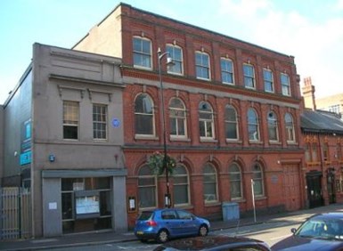
Figure 13 - Original site of the Elkington Plating Works in Birmingham, England, circa 2012.
Holding a virtual monopoly with the gold and silver electroplating patent rights, the Elkington Plating Works prospered significantly from the original Wright patent and enjoyed the rights and privileges the patent afforded to them for the years of its exclusivity. Thus, with a head start over others in the field of commercial decorative electroplating, the Elkington Plating Works meteoric growth peaked with a workforce of some 1,000 employees by 1890.12 Its original building still stands today in Birmingham (Fig. 13).1,9
The Woolrich Generator
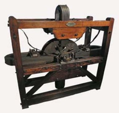
Figure 14 - Woolrich Generator Birmingham Science Museum, Birmingham, England.
Since the voltaic pile was essentially a battery, its disadvantage would be the loss of D.C. current and an interruption to the plating cycle when its anodic material depleted. By 1844, the voltaic pile was replaced by a more reliable D.C. power source, the Woolrich Generator.9
In 1842, chemist John Stephen Woolrich, patented his idea for a D.C. electrical generator (Fig. 14). Two years later in February 1844 his newly created company, The Magneto Works Co., sold its first D.C. generator to the Birmingham tableware company, Thomas Prime & Sons, for the silver electroplating of tableware and hollowware (Fig. 15).

Figure 15 - Thomas Prime & Sons advertisement.10
The Woolrich generator was a magneto-type generator using permanent magnets to create the magnetic field in which the windings rotate. In contrast, most generators use electromagnets in which a current flows through a coil to create the magnet field. Electromagnets can produce stronger fields and importantly, the field can be varied to adjust the voltage generated. Electroplating requires a direct current, so the Woolrich generator was fitted with an early commutator.
Nickel as a Replacement for Silver Plate
Dr. R. Bottger & the First Nickel Bath
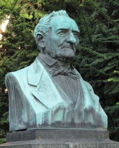
Figure 16 - Dr. Rudolf Böttger (1806-1881).
About this time, 1840-1844, an interest developed in the replacement of silver electroplate with nickel electroplate. The primary advantage was that nickel was less expensive to purchase than silver. Then, as is now, overhead cost savings were an important part of any business’ profitability.
In 1843, German scientist at the University of Frankfurt am Main; turned electroplater, Dr. Rudolf Böttger (Fig. 16), developed the first practical formulation for the electroplating of nickel while researching an electrotyping process for printing press plates.2,4 Böttger’s aqueous solution of nickel and ammonium sulfate remained the basic nickel electroplating formulation for the next 25 years.
William H. Remington Anode Baskets
In Boston, MA in 1866, businessman William H. Remington additionally realized a second advantage to nickel electroplating versus silver electroplating; that being a nickel electroplated coating could be buffed to a mirror reflective condition.1 Due to its anti-corrosive properties, the nickel coating would remain bright, reflective and lustrous, whereas silver and silver electroplate had to be routinely buffed as they continuously tarnish. That year, Remington established the William H. Remington Co. for the decorative electroplating of nickel and silver.4 Remington contributed to the advancement of the science, with his 1868 invention of the anode basket. Remington received U.S. Patent No. 82,877 in Oct. 1868 for the device.
Dr. Isaac Adams; Job Shop Nickel
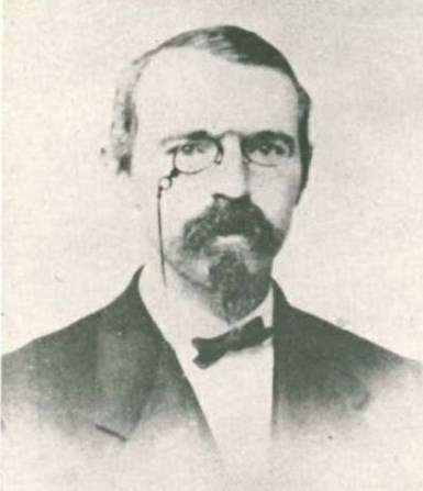
Figure 17 - Dr. Isaac Adams Jr.; 1836-1911.
Born in Boston, MA in 1836, Isaac Adams Jr. (Fig. 17) graduated Bowdoin College in 1858.4 He then attended Harvard Medical School receiving his M.D. in 1862, which he followed with two additional years of study at the Êcole de Médicine in France. Returning to Boston, he opened a medical practice, then abandoned it in 1866.
He opened a chemistry laboratory in Boston and delved into the topic of the day for electroplaters - the advancement of nickel electroplating. Employing Dr. Rudolf Böttger’s nickel plating bath of 1843, in just three years of experimentation (Fig. 18), Dr. Adams developed an improved nickel electroplating procedure.4

Figure 18 - Notes from Dr. Adams’ laboratory notebook from July 26, 1866.
Dr. Adams received U.S. Patent No. 98,157 on August 8, 1869, for “Improvements to the Electro-Deposition of Nickel.”4 In his improved bath, Adams substituted the double salt of nickel ammonium sulfate for Böttger’s use of the single salt of ammonium sulfate. This enhanced bath performance, providing additional nickel cations for deposition. Adams also determined that maintaining the bath at a pH value at 4.04,8 with the periodic addition of sulfuric acid would enhance performance.
At pH 4, Adams minimized ammonium hydroxide formation, the result of oxygen generation at the anode. Higher pH values, he found, lowered cathode efficiency and embrittled the nickel. In 1869, with patent in hand, Adams purchased the William H. Remington Co. in Boston, renamed it the Boston Nickel Plating Co.,1,4 and employed his new nickel plating bath, while also continuing to commercially electroplate silver on a job shop basis.
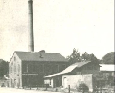
Figure 19 - The former Adams Plating & Mfg. Co. in South Windham, CT circa 1954.1,4
In 1872, he opened the first, commercial, exclusively nickel-plating job shop in the U.S. The Adams Plating & Manufacturing Co. was located in the town of South Windham, CT (Fig. 19).4 Dr. Adams also adopted Remington’s use of anode baskets to hold the bath’s anodes. Dr. Isaac Adams Jr. is credited with being the father of nickel plating in the United States.4,8
Dr. Edward Weston and Boric Acid
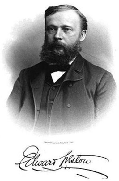
Figure 20 - Dr. Edward Weston circa 1870.
Born in England in 1850, Dr. Edward Weston (Fig. 20), like Dr. Adams, also trained as a physician, but abandoned his medical training. Landing in New York City in 1870, he too soon began experimenting with nickel electroplating improvements.4,5 Unable to determine an end-around to bypass Adams’ patent, Weston was nonetheless the first person to introduce boric acid into a nickel plating bath to minimize nickel oxide formation. His technology was awarded a U.S. patent in 1878.1,4
Dr. Wilhelm Pfanhauser and Chloride
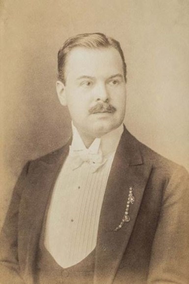
Figure 21 - Dr. William Pfanhauser circa 1900.
Working on further improvements to the nickel plating bath in Austria, Dr. Wilhelm Pfanhauser (Fig. 21), published in 1900, his work on nickel plating baths wherein ammonium chloride was added to the bath.4 Dr. Pfanhauser found that the addition of chloride to the bath, aided in nickel anode corrosion. By increasing the corrosion rate, he found that more dissolved nickel metal would be available in the bath. This of course increased the efficiency of deposition.
Dr. O.P. Watts and the Watts Plating Bath
Into this cacophony of emerging research, patent filings, legal patent defense claims, the use of boric acid to maintain pH and the recognition of chloride salts as an anode corrosion enhancement tool, stepped Dr. O.P. Watts at the University of Wisconsin (Fig. 22).2-4,7,11-14
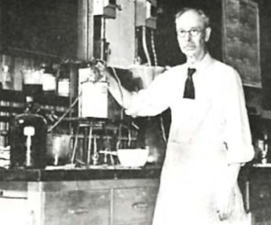
Figure 22 - Dr. Oliver P. Watts in his laboratory in the Electrochemistry Department at the University of Wisconsin, circa 1945.1,4
Having received his Ph.D. in 1905 from the University of Wisconsin, Dr. Watts spent the next 11 years tinkering with cobalt initially, but later with nickel plating baths. His landmark paper; “Rapid Nickel Plating,” was published in the Transactions of the American Electrochemical Society in April, 1916.4,7 With the publication of this paper, the blueprint was laid for the truly modern nickel plating bath, the bath that is most commonly in use around the world today. Today, the modern nickel plating bath is known as the Watts nickel bath in Dr. Watts’ honor (Table 2).4,5,7,8,13
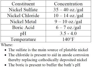
Table 2 - Typical Make-up of a Watts Nickel Plating Bath.2,3,7,11-13,15-18
Taking advantage of Weston’s previous discovery of boric acid to maintain nickel bath pH and Pfanhauser’s 1900 addition of chloride salts to foster anode corrosion, Dr. Watts’ made two significant breakthroughs.4 First, he elevated the nickel bath’s operating temperature and secondly, he realized that he could substitute nickel chloride for ammonium chloride to maintain good anode corrosion.
A galvanic cell carries electrical current efficiently when there are sufficient dissolved salts in solution to conduct the current. Using nickel chloride for anode corrosion not only increased the amount of nickel cations available for deposition, but additionally maintained the chloride anion for anode dissolution. As a result of these changes, the Watts nickel plating bath has a much higher level of dissolved nickel salts when compared to the earlier nickel baths of Böttger and Adams.2-4,7,12,15
Elevating the bath’s operating temperature to 140°F, and even as high as 160°F in some applications, coupled with the higher concentration of dissolved nickel salts for electrical efficiency, Dr. Watts created a nickel bath that could accept a much higher applied D.C. electrical current without cathode D.C. burn.4,5,13,19 Additionally, the higher concentration of salts permitted an increase of throwing power in low current density areas. By increasing current in the bath, Dr. Watts was able to deposit more nickel per hour in his bath in accordance with Faraday’s First Law.3,7,8 Looked at from a different angle, Dr. Watts was able to achieve a desired nickel thickness more rapidly because the bath was more electrolytically efficient.1
Bright Nickel Plating
Semi-bright nickel deposits are bright but not reflective. The deposits are white, matte and malleable.3,4,5,7,15 Prior to the introduction of brightening agents to the nickel plating bath, this matte and malleable nickel deposit would have to be hand-buffed to achieve a mirror-reflective finish. This was prior to the introduction of chromium plating to meet the rise in the popularity of automotive bright trim in the 1930s.3,7,8,20 Considering the cost of the hand labor, even in the late 1920s and early 1930s, required to achieve the improved mirror-reflective finish, the search was on to develop a nickel bath capable of generating a mirror-reflective appearance as the nickel was being deposited.8
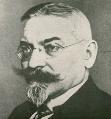
Figure 23 - Entrepreneur Max Schloetter, 1879-1946.
Working at the plating supply company he founded in Berlin, Germany in 1912, scientist and entrepreneur Max Schloetter (Fig. 23), discovered in 1930 that the introduction of the organic aromatic sulfonate compound, sodium benzene disulfonate (Fig. 24), would generate a dramatically improved, hard, smooth, mirror-reflective finish to what was formerly a semi-bright nickel plated deposit.2-4,7,8
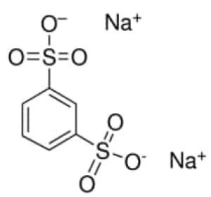
Figure 24 - The first secondary nickel brightener, sodium benzene disulfonate.
In 1932, Schloetter filed for a U.S. Patent and in 1933 he was granted U.S. Patent No. 1,972,693 for his bright nickel plating additive.4 He began advertising his bright nickel plating process in assorted German trade journals on December 1, 1933. In 1934, Schloetter sold the rights to the Schloetter Process to The Pyrene Manufacturing Co. in the U.S., which began marketing the first practical bright nickel plating bath as Pyrene High Gloss Nickel in 1934.4,8
Also in 1934, Mr. Virgil Waite, with the McGean Chemical Co. filed a patent on the use of aromatic sulfonates coupled with the use of cadmium and/or zinc as brightening agents.16 This development was the first of the bright nickel solutions better known today in which separately added control agents and brightening agents are added to the bath.
The Electroplaters’ Society
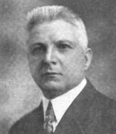
Figure 25 - Association Founder Charles Henry Proctor.6,14
In the early 1900s, in Arlington, NJ, Charles Henry Proctor (Fig. 25) was employed at the F.H. Lovell Foundry as the company’s electroplating foreman and foundry supervisor. At the time, the F.H. Lovell Foundry was widely recognized for forging then decoratively finishing a wide assortment of fixtures for passenger steamship staterooms and luxury Pullman railway cars. Attractive lighting fixtures, air grates and such were forged and decoratively plated at F.H. Lovell Foundry. Proctor was responsible for those efforts.
On March 6, 1909, Charles Henry Proctor, achieved his long, desired a dream and inspired a meeting of some two-dozen foremen platers.13 The group held their first meeting at the old Hotel Chelsea in New York City (Fig. 26).

Figure 26 - Chelsea Hotel, NYC, circa 1920.21
The purpose of which was to create a non-profit association to foster the advancement of electroplating, metal finishing and allied arts.13 Out of their thinking and planning, the National Electroplaters Association of the United States and Canada was formalized or NEPA, came into being at an organizational meeting held at the same Chelsea Hotel on Saturday, April 10, 1909.
NEPA Logo
For his organizational efforts and prescience members selected Charles Henry Proctor, NEPA president. Proctor presided at that first meeting, at which the infant organization approved its constitution and by-laws.13 The 60 charter members at this meeting were a doubling of the number present at the meeting; just one month previously. NEPA was incorporated as a New York Corporation on October 18, 1909.
From its inception, NEPA was a technical-educational society with its principal reasons being:
- “To advance and disseminate knowledge concerning the art of electrode-position of metals.
- To maintain a laboratory equipped for research work.
- To conduct meetings for the purpose of presenting papers on appropriate technical and scientific subjects and
- To publish technical literature.”
The first NEPA Banquet was held January 15, 1910. By 1912, NEPA became an international organization, chartering a branch in Toronto, Ontario. NEPA’s third annual banquet in 1912 featured the first exhibit of suppliers’ products. It was the granddaddy and precursor to today’s SUR/FIN conferences.1
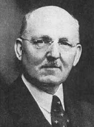
Figure 27 - AES First President George B. Hogaboom
In 1913, NEPA was reorganized and adopted as its name the American Electroplaters’ Society or AES. The reorganization was made to further meet its mission and to grow membership. At the 1913 Annual Banquet, the AES constitution and by-laws were adopted and George B. Hogaboom (Fig. 27), a NEPA charter member and electroplating foreman at the Scovill Manufacturing Co. in Waterbury, CT was elected the first AES president. 13
George B. Hogaboom; is best remembered for co-authoring with Dr. William Blum, the electroplater primer still used today entitled The Principles of Electroplating and Electroforming.11
AES Logo 1913-1985
AES remained the legacy society for 72-years and adopted as its logo, the three inter-twined AES letters surrounded by the society’s name American Electroplaters’ Society.
By 1985, the society morphed yet again. In recognition of the society’s 75th anniversary or “Diamond Jubilee;” as well as the changing work environment of membership which had expanded beyond just electroplaters and now consisted of individuals who were involved in all aspects of surface finishing, the society’s name and logo were changed yet again.
The society’s new name was the American Electroplaters’ and Surface Finishers Society; or more conveniently just AESF.
AES Logo 1985-2007
The new logo included the society’s AESF moniker; in gold font, atop of a stylized blue diamond background; symbolic of the legacy society’s diamond jubilee.1
With the advent of personal computers, the availability of information online, the diminishing influence of “old timers” and the increase in retirees there came a diminution in societal attendance at the branch and national meetings. Falling membership levels accompanied by plummeting income lost as membership dues were lost lead to a near bankruptcy of the society by the mid-2000s. However, a dedicated team of AESF loyalists, who understood the historical significance of the society and the camaraderie of fellow membership, were able to reorganize the society into its current format.
In 2007, AESF was reorganized as the National Association for Surface Finishing or NASF, as it simultaneously merged with the NAMF, National Association of Metal Finishers and the MFSA, Metal Finishing Suppliers Association. Both the NAMF and the MFSA, proud legacy equals to the AESF, were suffering from the same membership ills. It seemed and remains a logical merger of the societies all of which have as a common core; metal finishing.
Current NASF and AESF Foundation Logos 2007-Present
A new NASF logo was adopted and the AESF Foundation was formed to serve as the society’s educational bulwark. The AESF Foundation serves as the Society’s educational arm to this day.
References
- William P. Nebiolo, “The History of Electroplating,” presentation at NASF New England Regional; Salem, MA; 2017.
- George A DiBari, Practical Nickel Plating: An AES Illustrated Lecture, The American Electroplaters’ Society Inc., Newark, NJ; 1973; pp. 1-30.
- George A. DiBari and R.A. Covert, Nickel Electroplating: An AESF Educational Course; The American Electroplaters and Surface Finishers Society, Orlando, FL; 1992; pp. 1-32.
- George Dubpernell, “The Story of Nickel Plating”; Plating, 46 (6), 599-616 (1959).
- R.J. McKay, “The History of Nickel Plating Developments in the U.S.A., Part I,” Plating, 38 (1), 41-44, 57 (1951).
- Flavio J. LaManna, The Fundamentals of Chemistry for Electroplaters; Electroplating Course Manual; Chapter 2, The Newark Branch of the American Electroplaters’ Society, 1980.
- George A. DiBari, “Electrodeposition of Nickel”, Modern Electroplating, Chapter 3, edited by M. Schlesinger and M. Paunovic, John Wiley & Sons, Inc., New Jersey; 2010; pp. 79-114.
- R.J. McKay, “The History of Nickel Plating Developments in the U.S.A., Part II,” Plating, 38 (2), 147-156 (1951).1. Blum, William PhD, Hogaboom, G.B.; “Principles of Electroplating and Electroforming”; 3rd Edition; 1949; McGraw-Hill Book Co.
- Grace’s Guide to British Industrial History, https://www.gracesguide.co.uk/Elkington_and_Co, 2017.
- B. Giorio, www.silvercollection.it, Englaprime, Thomas Prime & Sons, 2017.
- William Blum, and G.B. Hogaboom, Principles of Electroplating and Electroforming, 3rd Edition, McGraw-Hill Book Co., New York, 1949.
- Warren H. McMullen, “Chapter 8: Nickel Plating”; Electroplating Course Manual: Basic Practical Electroplating, Edition No. 8; The Newark Branch of The American Electroplaters’ Society; 1980; pp. 110-129.
- John P. Nichols, “Kaleidoscope of AES’s First Half Century,” Plating, 46 (6), 650 (1959).
- The Metal Industry Co., The Metal Industry, 5, 167 (June 1907).
- Harold J. Read, and R. Weil, “Grain Size and Hardness of Nickel Plate as Related to Brightness,” Plating, 37 (12), 1257-1261 (1950).
- Arthur H. DuRose, The 11th William Blum Lecture, 57th Annual Convention of the American Electroplaters’ Society, June 22, 1970, Montréal, Québec
- L. Oniciu and L. Muresan, “Some Fundamental Aspects of Leveling and Brightening of Metal Electrodeposition,” J. Applied Electrochemistry, 21 (29), 565-574 (1991).
- Edward B. Saubestre, “The Chemistry of Watts Nickel Plating Solutions,” Plating, 45 (9), 927-936 (1958).
- Louis Gianelos, “Troubleshooting of Nickel Plating Solutions (AES Update: Part I of III: Part Series on Nickel),” Plating & Surface Finishing, 64 (8), 32-34 (1977).
- Edward B. Saubestre, “The Chemistry of Bright Nickel Plating Solutions,” Plating, 45 (12), 1219-1227 (1958).
- Maude Gonne, New York as it Was, Pinterest web pin, New York City Historic Buildings, 2018.
About the author

William P. Nebiolo received a B.A. degree from The University of Connecticut and an M.S. degree from Long Island University. Bill began his metal finishing career at Union Hardware Div. Brunswick Sporting Goods as a plating lab technician. After 2-years at Eyelet Specialty Co. as a plating foreman, 5-years at Nutmeg Chemical as the laboratory director and 3-years at The Stanley Works Corporate Laboratory as chief electrochemist, Bill accepted a position at REM Chemicals, Inc. in Southington, CT as a sales engineer in 1989. He remains at REM to this day, currently serving as Sales Engineer for REM's Midwestern Sales Territory and as REM’s Product Manager.
He joined the NASF as a member of the Waterbury Branch of AES in 1978. Working his way through the branch officers’ chairs, Bill served as Waterbury Branch President 1984-85 and was appointed Branch Secretary in 1991. Bill spearheaded the merger of the Waterbury, Bridgeport and Hartford Branches into the Connecticut Branch in 2004, then petitioned and was awarded branch certification through AESF National. Bill was immediately appointed Connecticut Branch Secretary and remains in the role to this day. He has represented the Connecticut Branch as an NASF National Delegate, has served as a technical chair at several NASF SUR/FIN technical sessions was awarded an NASF National Award of Merit in 2010 and in 2012 was elevated to the position of Connecticut Branch Honorary member. He served on the NASF Technical Advisory Board for many years, becoming the Chair in 2021.
To date, Bill has published a dozen papers in assorted technical journals and presented more than 20 papers at technical conferences and seminars. From 1996 – 2000 Bill served as one of SME’s Mass Finishing Technical Training Program instructors at more than two dozen training sessions. Bill is the author of the SME Mass Finishing Training Book and the REM Training Manual which is now in its 8th edition.
* Corresponding author:
William P. Nebiolo
REM Surface Engineering
325 West Queen Street
Southington, CT 06489
Phone: (860) 621-6755
Cell: (860) 985-3758
E-mail: bnebiolo@remchem.com
A Lifelong Partner for the Surface Finishing Industry
Products Finishing magazine has served the surface finishing industry since its inaugural issue was published in October of 1936. Here, inspired by Mr. Neblio’s fascinating look into the history of the electroplating industry, is a look back at the publication’s 50th anniversary through the words of longtime PF editor-in-chief Jerry Poll.


Images: From the archives of Products Finishing
Today, more than 85 years since its first issue, PF’s mission continues as much more than a singular magazine (though we’ll admit those original digest-sized journals are a delight to hold), but a media brand offering a wide variety of platforms to help educate and inform those in the surface finishing community.
As we look ahead to what is in store for the finishing industry, the goal of PF is to help serve the needs of those in this community as a lifelong partner. Cheers to the future!
RELATED CONTENT
-
Evaluation of Atmospheric Corrosion on Electroplated Zinc and Zinc-Nickel Coatings by Electrical Resistance (ER) Monitoring
This paper is a peer-reviewed and edited version of a presentation delivered at NASF Sur/Fin 2013 in Rosemont, Ill., on June 12, 2013.
-
Cyanide-Free Electroplating of Cu-Sn Alloys
This paper is a peer-reviewed and edited version of a presentation delivered at NASF SUR/FIN 2012 in Las Vegas, Nev., on June 13, 2012.
-
Development of a Sustainability Metrics System and a Technical Solution Method for Sustainable Metal Finishing: AESF Research Project #R-121, 6th Quarterly Report
The NASF Research Board has funded a research grant at Wayne State University on sustainability in the surface finishing industry, under the direction of Professor Yinlun Huang. The objective of the work is to create a surface-finishing-specific sustainability metrics system to measure economic, environmental and social sustainability. In this report, a benchmarking study of five plants was undertaken to illustrate how the sustainability assessment works.