Crack Formation During Electrodeposition and Post-Deposition Aging of Thin Film Coatings - 13th-14th Quarter Report
This NASF-AESF Foundation research project report covers the 13th and 14th quarters of project work (January-June 2019) on this AESF Foundation Research project at the University of Houston. The activities in this period continued towards calculating an optimum pulse current deposition method to control and mitigate the stress state of chromium thin films. This study should enable development of an effective strategy generally applicable in practice whenever electrodeposition process for crack-free films is demanded.
#nasf
Editor’s Note: This NASF-AESF Foundation research project report covers the 13th and 14th quarters of project work (January-June 2019) on the AESF Foundation Research project at the University of Houston. Access information to past project reports referred to in this paper is listed at the end of this report. A printable PDF version of this report is available by clicking HERE.
Objective: The objective of the work is to study fundamental and practical aspects of crack formation in electrodeposited thin films. The aim is to identify and quantify the key parameters of the electrodeposition process affecting the crack formation in thin films. This study should enable development of an effective strategy generally applicable in practice whenever electrodeposition process for crack-free films is demanded. The activities in this period continued towards calculating an optimum pulse current deposition method to control and mitigate the stress state of chromium thin films. The chromium films were deposited from trivalent chromium (Cr+3)-containing electrolytes (EXDBA 1411 Bath with pH=5) using different pulse current functions and their stress state was compared to the ones deposited with DC current.
Featured Content
Experimental approach and results: In our previous reports, we discussed the origin of crack formation on films deposited from a trivalent chromium electrolyte. In such a coating, the film forms open cracks that are detrimental for many engineering applications. In general, there is a critical thickness above which thin films develop cracks. This thickness can be defined as:
(1)
in which A is a geometrical term, while E, Γf, and σm represent the elastic modulus of the film, the fracture toughness term, and tensile stress, respectively. It is important to note that only tensile stress can cause crack propagation while generally, compressive stress works against development of cracks.
In previous reports, we have shown that the stress state of chromium films deposited from Cr3+ electrolytes during the growth stage is compressive. This is due to formation of chromium hydride. Therefore, cracks in such films have a post-deposition origin, where unstable Cr-H formed during the deposition starts to decompose and consequently results in generation of a tensile stress.
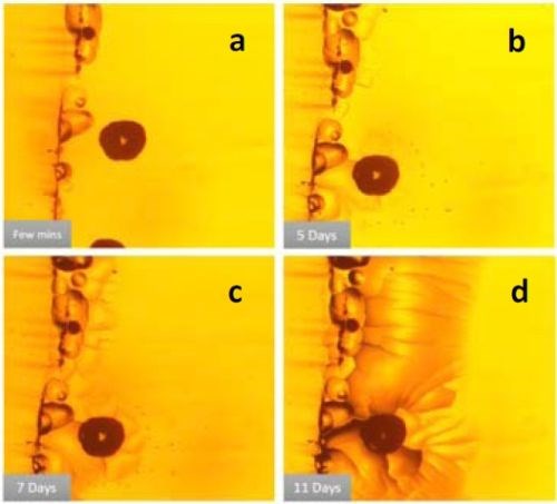
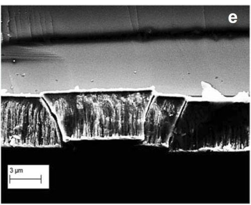
Figure 1- (a-d) Optical image of DC deposited chromium film using a Cr+3-based electrolyte, showing crack development over time; (e) cross-sectional SEM image of the cracked film.
Figure 1 shows the development of cracks after the deposition stage in chromium films deposited with direct current (DC) from a Cr+3 electrolyte. Figures 1(a-d) are optical images of a particular spot on a typical chromium film from immediately after deposition to about 11 days after the film growth. One can clearly notice the development of cracks over time. These cracks propagate in depth and on the surface and cause the mechanical integrity of the film to be compromised over time. Figure 1(e) shows a cross-sectional SEM image of the cracked chromium film. The figure shows how such cracks penetrate the entire thin film thickness, resulting in open-crack failure of the film.
To address this issue, we proposed a pulse current (PC) deposition approach, which allows the films to decompose chromium hydride and relax during the film growth stage. Based on our analysis, presented in the last report (http://short.pfonline.com/NASF19Feb1), the chromium hydride decomposition continuously occurs for a long period of time after deposition. However, it is only necessary to wait for about seven times the deposition time to decompose a significant portion of hydride and thus relax the film. The analysis suggests that designing pulse current deposition with X sec on and 7X sec off leads to films with a negligible hydride content. Such effective hydride removal during deposition essentially minimizes the tensile relaxation after the deposition, which is the driving force for the crack formation based on Equation 1. To validate this concept, we designed pulse currents with X sec on and various off-times (0 to 10X sec) and measured the tensile relaxation immediately after the film deposition.
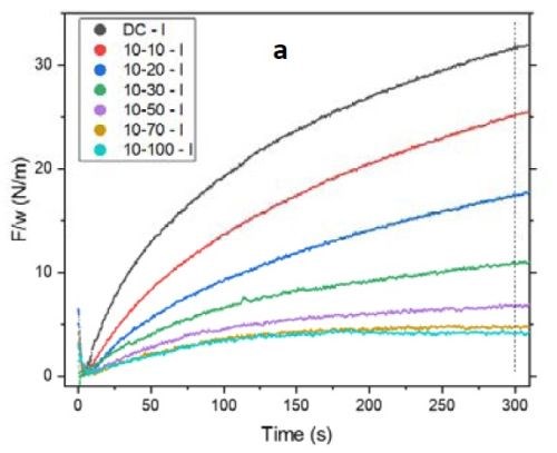
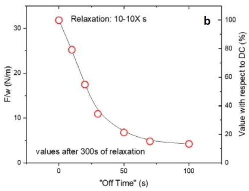
Figure 2 - (a) tensile relaxation transient (F/w vs. time) of films with the same thickness and on-time but with various off-times; (b) the value of F/w plotted after 300 sec from the beginning of the relaxation process.
Figure 2(a) shows the first 300 sec of the relaxation transient of the pulse current deposited films with 10 sec on and various off-times from 0 to 100 sec. To ensure that the relaxation behaviors of the films were comparable, all were deposited over 100 sec of net deposition time, which produces a constant thickness of ~135 nm. As expected, by increasing the off-time in the pulse function, the tensile relaxation after the deposition decreased and more readily reached steady state. However, increasing the off-time above 50 sec (5X) was not practical. The gains were almost negligible beyond 70 sec (7X) (Fig. 2(a)). This implies that the majority of the hydrides were decomposed after 7X off-time. These data are highly compatible with our analysis in the previous report where film relaxation at seven times the deposition-time was insignificant. Figure 2(b) shows the value of F/w after 300 sec relaxation of the deposited films. The right axis displays the percentage of those values with respect to a DC deposited film. It is obvious that the relaxation value in pulses with 7X off-time drops to 15% of the value observed for the DC sample. Further increase in the off-time to 10X reduces the tensile value by only an additional 2% and decreases the relaxation value to 13% of the DC film value. This is a small gain compared to the time added in the elongation of the entire duty cycle of the pulse current function.
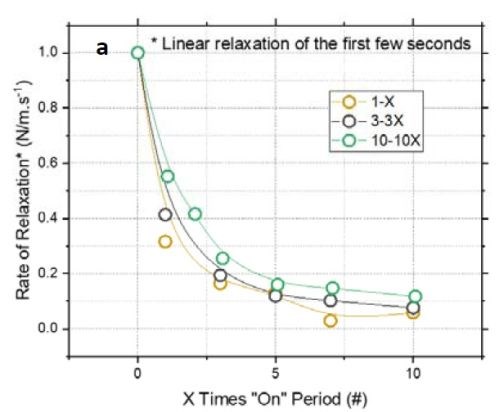
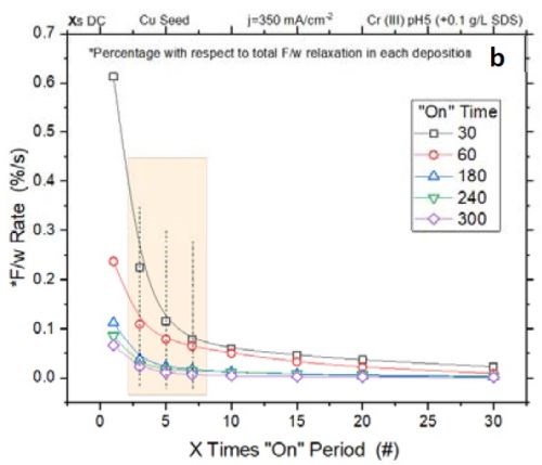
Figure 3 - (a) Normalized tensile relaxation rate of films deposited with various pulses immediately after the deposition; (b) F/w rate transient of films deposited with various on-times (thickness).
Figure 3(a) shows the normalized rate of relaxation immediately after deposition (N/m⸳sec-1) for films deposited with various pulse lengths and duty cycles.[1]** The initial rate of relaxation can indirectly indicate the content of chromium hydride in the film. A higher rate in the initial stage suggests more accumulated chromium hydride in the film, which starts to decompose immediately after deposition. For comparison, all films were deposited with the same thickness of 135 nm. The graph shows that independent of the deposition pulse length (X sec) - whether it is 1, 3 or 10 sec - the initial rate of relaxation follows the same trend as a function of the off-time. Employing pulses with off-times longer than 7X will not significantly reduce the rate of relaxation. Therefore, these data suggest that using pulses with more than 7X sec off-time only slightly helps in reducing the hydride content in the film. These results are also compatible with Fig 3(b), which shows that the relaxation rate will decrease after 7X.
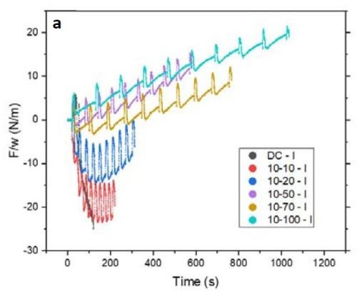
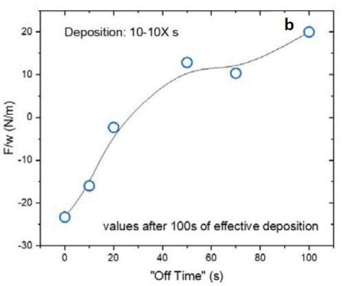
Figure 4 - (a) F/w transient of the films with 10 sec on and various duty cycles during the deposition stage; (b) value of F/w from (a) after 100 sec (135 nm) of deposition.
Figure 4(a) is plot of the F/w transient of the respective films deposited with 10 sec on and various off-times from 0 to 100 sec (or a duty cycle of 100 to 9%) during the growth stage. Inserting a periodic off-time after each 10 sec of deposition clearly can change the F/w (stress) state of the film from compressive to tensile. Figure 4(b) summarizes the values of F/w after 100 sec of net deposition (~135 nm). This graph shows that employing an off-time of more than 20 sec (2X) puts the film under tensile stress during the growth stage. This is characteristic of films deposited from a hexavalent (Cr+6) electrolyte. In this case the contribution of grain boundary zipping dominates the stress state of the film as compared to the compression from the chromium hydride.
It is important to mention that the film data presented in Fig. 4(a) are in an initial stage of growth. For a more conclusive analysis on the stress state of the film during the growth, it is better to deposit a thicker film where film growth is at steady state.
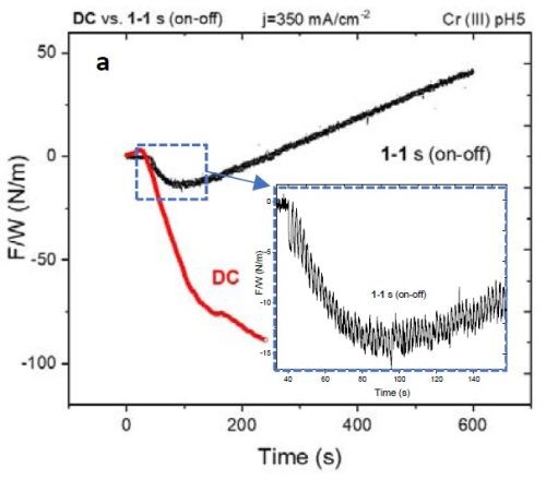
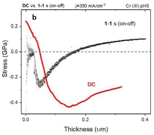
Figure 5 - (a) F/w transient of the DC vs. PC (1 sec on - 1 sec off) deposited films. The inset shows compression during the early stage of film growth; (b) stress-thickness graph of the films in (a).
Figure 5(a) shows the F/w transient of samples with DC and PC (1 sec on - 1 sec off; 50% duty cycle) deposition of ~400 nm thickness. Over the deposition-time, the F/w value in the PC-deposited film shows a steady tensile F/w increase, while at an early stage in the deposition (inset of Fig. 5(a) and 10 sec on - 10 sec off in Fig. 4(a)) the film exhibits compression. This transition can suggest that, at an early stage of growth, the contributors of compressive stress, such as chromium hydride formation and Laplacian pressure on the grains, are dominant players in determining the net stress of the film. At this early growth stage (Fig. 4), grain merging as a contributor to tensile stress is not effective where nuclei forming on the surface are widely scattered. However, Fig. 5(b) shows the stress vs. thickness relationship of the same films. Clearly, the stress state of the films deposited with DC and 1 sec on - 1 sec off pulse show a dramatic difference, where the DC films remained in compression during film growth, while the pulsed deposit developed a tensile stress in the later stage of deposition. To study if employing pulse deposition can also change the film composition and morphology, we obtained STEM-HAADF images and used an EDS detector to obtain a chemical map of the deposited films.
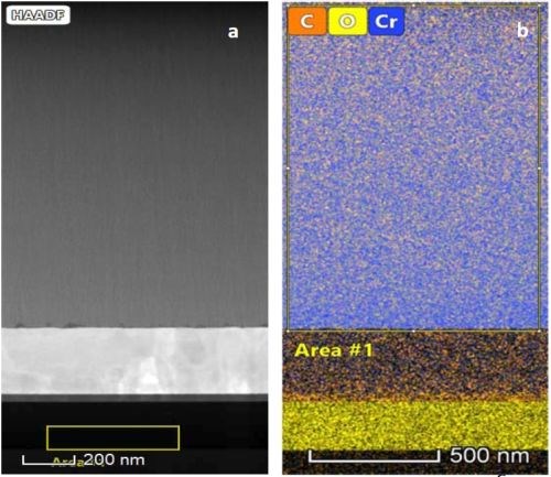
Figure 6 - (a) STEM-HAADF image of the DC deposited film; (b) chemical map of the same film obtained using an EDS detector.
Figure 6(a) shows the STEM-HAADF images of a typical DC deposited film. The film shows no crystalline or observable grains. Figure 6(b) shows the chemical map of the same deposit. The film shows uniform distribution of the chromium, oxygen and carbon over the entire film. The chemical percentage of the selected Area #1 is summarized in Table 1.
Table 1 - Chemical composition of the selected area of the DC-deposited film shown in Fig. 6(b).
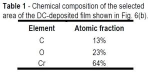
Table 1 shows a significant oxygen content (23%) in the film, which suggests formation of chromium hydroxide and/or chromium oxide during film growth. These assumptions are bolstered with EELS data (not presented in this report), which show the presence of trivalent chromium in the deposited film. This valence cannot belong to the metallic state of chromium and is indicative of the presence of Cr(OH)3 or Cr2O3 oxide phases. These data supplement our analysis in the 6th Quarterly Report (see list below), which shows that the high hydrogen reduction rate at the cathode interface locally increases the pH. High pH at the cathode causes Cr(OH)3 to precipitate and, after exposure to air, it is detected as Cr2O3. The latter clearly reflects on the content of oxygen in the film. Incorporation of chromium oxide and hydroxide as a brittle phase is important, as they can adversely affect the fracture toughness of the deposits and make them more susceptible to crack formation (Equation 1).
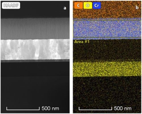
Figure 7 - (a) STEM-HAADF image of the PC (1 sec on – 1 sec off) deposited film; (b) chemical map of the same film obtained using an EDS detector.
|
|
Figure 7(a) shows STEM-HAADF images of film deposited with 1 sec on - 1 sec off pulse current. Figure 7(b) shows the uniform chemical map of the film in Figure 7(a). The chemical composition of the selected area is shown in Table 2.
Table 2 - Chemical composition of the selected area of the PC-deposited film shown in Fig. 7(b).
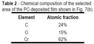
Comparing the chemical compositions of the DC-deposited film (Table 1) and the PC-deposited film (Table 2), the DC film shows significantly higher oxygen content (~+5.0%).
The reduced oxygen content in the PC film is related to the periodic off-time during the growth stage that allowed the pH of the solution at the interface to recover and become less alkaline. Note the higher carbon content in the PC-deposited film. This increase of carbon suggests more carbon incorporation most probably arose from the HCOOH ligand in solution. Another possibility may come from the TEM sample preparation procedure, where sputtered carbon is used to bond the sample to the TEM grid. Higher content of the carbon in the PC-deposited films needs further study for a more conclusive result.
Films with such amounts of impurities are expected to have a lower elastic modulus as compared to pure metallic films (~285 GPa).2 Figure 8 shows nanoindentation results for DC and PC-deposited films. Using nanoindentation enables us not only to measure sample hardness, but also to measure the elastic modulus of the film.
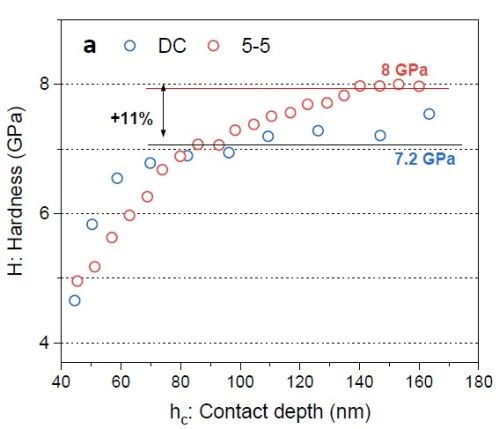
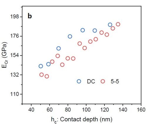
Figure 8 - (a) Hardness vs. contact depth for films deposited via DC and PC with 5 sec on - 5 sec off; (b) elastic modulus of chromium as a function of contact depth.
Figure 8(a) shows preliminary nano-hardness data. In the nano-hardness test, a Berkovich indenter is used and data interpretation is based on the applied load causing tip penetration in the film. By increasing the load, the penetration depth also increases. Based on the value for the load and the respective trace area that the indenter leaves in the sample, hardness data*** vs. contact depth was plotted. One can see that employing pulse current deposition can improve the hardness value (+11%). However, for a conclusive result, there is a need for more experimental study and statistical analysis. Figure 8(b) plots the chromium film elastic modulus as a function of the indenter contact depth. This modulus was calculated by knowing the elastic modulus of the indenter (Er) and Poisson’s ratio of chromium and the indenter.† The elastic modulus of the chromium film from the Cr3+ electrolyte was found to be about 165 GPa. This value is less than the elastic modulus of pure bulk chromium (~285 GPa) and also less than typical chromium films deposited from a hexavalent electrolyte (>170 GPa).2,3 This is because various phases are present as impurities incorporated in chromium film during the deposition stage. Based on Equation 1, reduction of the elastic modulus also makes sample more prone to crack formation.
Summary
Electrodeposited chromium films from trivalent chromium electrolytes are susceptible to crack formation. Three important parameters that can change the critical thickness to form through-film cracks are elastic modulus (E), fracture toughness (Γf), and the tensile stress (σm). Our studies and discussion show that, due to the presence of second phases and impurities, E and Γf have lower values as compared to pure metallic chromium films. This means that the most effective way to address chromium cracking is to handle the tensile stress that develops in the film after deposition. Pulse current deposition, with a proper pulse design can not only reduce the tensile stress in the film after deposition, but it also can slightly the improve fracture toughness of the film by reducing the overall content of oxygen. Figure 9 shows a typical DC vs. PC (1 sec on - 5 sec off) films one year after they were deposited. The photos clearly demonstrate that by employing a pulse current approach with no change in the bath chemistry or operating conditions, crack formation in chromium films can be dramatically reduced.
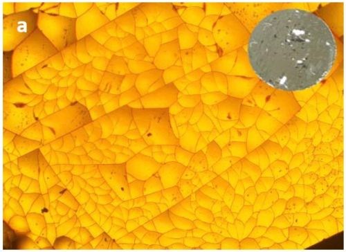
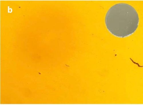
Figure 9 - 5× optical images of 5 μm chromium films one year after their preparation: (a) DC-deposited and (b) PC-deposited (1 sec on - 5 sec off). The top right corner of the images shows the actual appearance of the film.
References
1. L. B. Freund and S. Suresh, Thin Film Materials: Stress, Defect Formation, and Surface Evolution, Cambridge University Press, (2003); p. 283.
2. M.F. Ashby and D.R.H. Jones, Engineering Materials 1: An Introduction to Properties, Applications and Design (Vol. 1), Elsevier, (2012); pp. 38-39.
3. A. Brenner, P. Burkhead and C. Jennings, “Physical Properties of Electrodeposited Chromium” J. Research Nat’l. Bur. Std., 40, 31-58 (1948).
Past project reports
1. Quarter 1 (January-March 2016): Summary: NASF Report in Products Finishing; NASF Surface Technology White Papers, 81 (2), 12 (November 2016); http://short.pfonline.com/NASF16Nov2.
2. Quarter 2 (April-June 2016): Summary: NASF Report in Products Finishing; NASF Surface Technology White Papers, 81 (3), 14 (December 2016); http://short.pfonline.com/NASF16Dec2.
3. Quarter 3 (July-September 2016): Summary: NASF Report in Products Finishing; NASF Surface Technology White Papers, 81 (4), 12 (January 2017); http://short.pfonline.com/NASF17Jan2.
4. Quarter 4 (October-December 2016): Summary: NASF Report in Products Finishing; NASF Surface Technology White Papers, 81 (8), 16 (May 2017); http://short.pfonline.com/NASF17May2.
5. Quarter 5 (January-March 2017): Summary: NASF Report in Products Finishing; NASF Surface Technology White Papers, 81 (11), 12 (August 2017); http://short.pfonline.com/NASF17Aug1.
6. Quarter 6 (April-June 2017): Summary: NASF Report in Products Finishing; NASF Surface Technology White Papers, 82 (4), 10 (January 2018); http://short.pfonline.com/NASF17Jan1.
7. Quarters 7-8 (July-December 2017): Summary: NASF Report in Products Finishing; NASF Surface Technology White Papers, 82 (9), 10 (June 2018); http://short.pfonline.com/NASF18Jun1.
8. Quarters 9-10 (January-June 2018): Summary: NASF Technical Papers in Products Finishing; NASF Surface Technology White Papers, 83 (2), 17 (November 2018); http://short.pfonline.com/NASF18Nov1.
9. Quarters 11-12 (July-December 2018): Summary: NASF Technical Papers in Products Finishing; NASF Surface Technology White Papers, 83 (5), 11 (February 2019); http://short.pfonline.com/NASF19Feb1
About the authors

Dr. Stanko R. Brankovic is a Professor in the Electrical & Computer Engineering and Chemical & Biomolecular Engineering Departments, as well as Associate Director, Center for Integrated Bio and Nanosystems at the University of Houston, Houston, Texas. He holds a B.E. in Chemical and Biochemical Engineering from the University of Belgrade, Serbia (1994) and a Ph.D. in the Science and Engineering of Materials from Arizona State University, Tempe, AZ (1999). He is active in many professional societies, including serving as Chair and member of the Electrodeposition Division Executive Committee of The Electrochemical Society (2006‐present) and as the Chair of the Electrochemical Material Science Division, The International Society of Electrochemistry (2015‐2017). His research interests include electrodeposition, thin films, electrocatalysis, sensors, corrosion and electrochemical material science and nanofabrication.

Kamyar Ahmadi is a doctoral student in Materials Engineering program at the University of Houston (UH). He obtained B.Sc. in Materials Science and Engineering from Iran University of Science and Technology (IUST) in 2014 before he joined UH. His research interests are thin film deposition and electrochemical fabrication of functional materials.
Footnotes:
*Corresponding author:
Dr. Stanko R. Brankovic
Associate Professor
Department of Electrical & Computer Engineering
Department of Chemical & Biomolecular Engineering
Department of Chemistry
N 308 Engineering Building 1
Houston, Texas 77204-4005
Phone: (713) 743-4409
Fax: (713) 743-4444
E-mail: srbrankovic@uh.edu
** Duty cycle %=tonton+toff×100
*** H = F/A(hc)
† 1/Er = 1-νCr2/ECr+1-νin2/Ein
RELATED CONTENT
-
Zinc Electroplating
Choosing the best process for your operation.
-
Sizing Heating and Cooling Coils
Why is it important for you to know this?
-
Nickel Electroplating
Applications, plating solutions, brighteners, good operating practices and troubleshooting.


