
Share
A Synopsis* of a Presentation given at SUR/FIN 2017 (Atlanta, Georgia)
by
Konstantin Schwarz
Atotech Deutschland GmBH
Berlin, Germany
and
Joseph Arnold**
Atotech USA, LLC
Rock Hill, South Carolina, USA
Editor’s Note: The following is a synopsis of a presentation given at NASF SUR/FIN 2017, in Atlanta, Georgia, on June 19, 2017 in Session 3, Technologies for Performance. This brief can be accessed and printed HERE; the complete Powerpoint presentation is available by clicking HERE.
Featured Content


ABSTRACT
A new combination of copper immersion and autocatalytic copper-(I)-oxide deposition enables lower palladium concentrations in the activator bath, though the amount of copper deposited on the plastic surface can be up to 10 times higher compared to its predecessors’ processes. This way, the dragout cost of palladium is further minimized. Also, the use of this new combination of copper deposition mechanisms enables a reduction in the surface resistivity of the resulting layer by a factor of about 10 compared to older direct metallization processes. Besides easier direct plating on large plastic surfaces and PC-ABS blends, one major advantage is the high stability of the new process.
Introduction
A primary goal in the development of plating process for ABS plastics is the simplify the process sequence, reducing the number of steps. In particular, eliminating the electroless nickel and/or copper strike steps through direct metallization has been important. Over the last two decades, research and development efforts at Atotech have worked toward this end, striving for high performance and reducing costs in direct metallization processes for ABS and ABS/PC. In this article a survey of a new proprietary state-of-the-art direct metallization system NeoLink®E was given by Mr. Joseph Arnold.
The Technology
As shown in Figure 1, the process involves a drop-in modification in the standard ABS process sequence following the etch, neutralization and catalyst activation steps. Instead of an electroless process, the original standard direct process used an adherent immersion copper coating (Cu-Link) to replace the tin layer. The new development involves a novel immersion deposit (NeoLink E) to produce a thick conductive layer of copper (by tin exchange) and promote autocatalytic growth of 200-nm copper oxide crystals on the surface, to allow direct electroplating of the decorative process sequence.

Figure 1 – Direct metallization process sequence.
The resulting layer is adherent, and is sufficiently conductive to allow the workpiece to directly enter the acid copper plating step with no further intermediate steps. The process is highly stable, requiring no chemical stabilizers. It is cost-efficient, easy-to-use and suitable for both small and large ABS and ABS/PC plastic parts. A comparison of the bold and new processes is shown in Figure 2

Figure 2 – Principle summary of direct metallization processes.
Test Results
The fact that tin in the activator layer is replaced by copper along with the development of copper oxide crystals makes for increased conductivity, as seen in Figure 3. Further, the activator can operate with reduced palladium content, reducing palladium dragout and operating at higher efficiency.


Figure 3 – Low resistivity / high conductivity on ABS and ABS-PC.
Production results
In production testing, it was shown that coverage increased, despite the reduction in palladium concentration (Figure 4). In the figure, it can be seen that full coverage is achieved with 30 ppm Pd with the immersion copper/copper oxide process. This contrasts with the conventional technology results shown, with 50 ppm Pd required for full coverage.


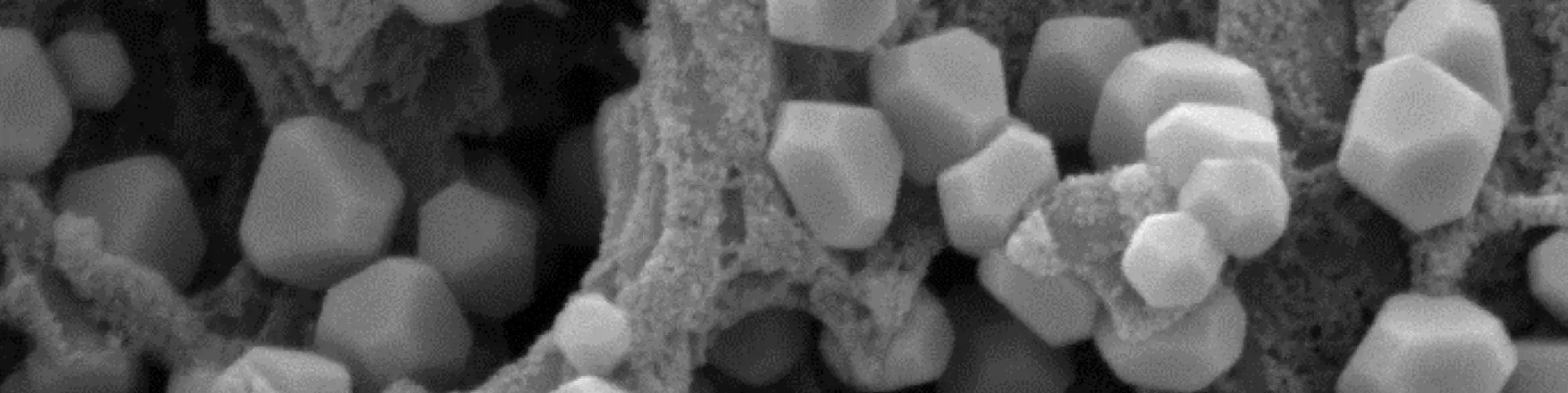
During the process time, there was no discernible increase in particle size of the copper oxide crystals. Rather, there was an increase in particle density, which continued for up to eight minutes deposition time (Figure 5). With this was an increase in layer conductivity.


Figure 5 – Effect of immersion time on the layer structure (Activator time - 5 min; immersion Cu/Cu oxide time 2, 4, 6, 8 min)
|
|
Of course, the primary concern for any plating-on-plastic application is plate adhesion. The OEM specifications for plate adhesion for a selection of manufacturers is shown in Fig. 6, based on a standard acid copper plate thickness of 30-40 μm.
Actual parts processed with the new immersion technology were tested and compared with standard technology as a reference. Values were comparable. An ABS cap showed an adhesion value of 14.2 N/cm (8.1 lbs/in) for the Neolink technology versus 14.8 N/cm (8.5 lb/in for the conventional processing, significantly higher than the OEM specs. An ABS-PC BMW Mini front panel processed with the immersion Cu/Cu oxide process showed an adhesion value of 7.3 N/cm (4.2 lbs/in) versus 7.2 N/cm (4.1 lbs/in) for conventional processing.

Figure 6 – OEM adhesion specifications for plated ABS and ABS-PC plastics (30-40 μm electrodeposited acid copper).
Summary
In summary, Mr. Arnold noted that operating costs for the new Neolink E technology were similar to those for conventional processing. Significantly thicker copper deposits were obtained on the plastic surface in the form of copper metal and copper oxide. No visible surface roughness was observed with the presence of Cu2O cuprous oxide particles in the layer. In production, a layer with higher surface conductivity was available prior to acid copper plating, and excellent coverage was achieved. In operation, the palladium concentration required in the activator solution was lower, leading to reduced dragout and lower costs. With no stabilizers needed, the solution was easy to use, and was suitable for both small and large parts molded from ABs and ABS-PC.
About the author / presenter
Konstantin Schwarz is worldwide manager special projects (DECO/POP), at Atotech Deutschland GmbH, Erasmustraße 20, 10553 Berlin, Germany.

Footnotes:
*Compiled by Dr. James H. Lindsay, NASF Technical Editor
** Presenter contact information:
Mr. Joseph Arnold
New Business Development Manager
Atotech, USA, LLC
Rock Hill, South Carolina
Phone:
E-mail: joe.arnold@atotech.com
RELATED CONTENT
-
Electroless Nickel-plated Steel versus Stainless Steel: Case Studies
This paper highlights two case studies of manufacturers that have replaced, or done studies to replace, stainless steel with electroless nickel-plated mild steel. In both cases, cost savings could be realized while maintaining or improving product quality.
-
Electroless Nickel Coatings: Appearance, Gloss and Surface Morphology
For decorative coatings, appearance is the essential purpose for application, but also for functional surface finishes it becomes increasingly relevant as an added value on top of specified technical requirements. Appearance is affected by spectrum and intensity of incident light, roughness and morphology of the coating surface, optical properties of the coating material, eventual superficial oxide films, and individual perception. The predominant factor is surface roughness, which in turn depends on base material roughness, quality of substrate pretreatment, and nucleation and growth kinetics of the electroless nickel (EN) deposit. Interdependency of gloss measurements with roughness measurements and with chemical composition of coatings was investigated for new generation mid-P EN processes and compared to traditional ones.
-
Methods and Formulas to Determine Internal Deposit Stress in Applied Metallic Coatings
Internal stress exists in electroplated and chemically applied metallic coatings. This paper reviews the test procedures for measuring deposit stress and the formulas used to calculate stress values. Many formulas used require modification to obtain actual internal stress values. Errors in this regard are examined and common mistakes are explained.


